Laser annealing device and method

a laser annealing and annealing device technology, applied in the direction of manufacturing tools, instruments, optical elements, etc., can solve the problems of non-ideal annealing effect, significant increase in annealing time, and ic fabrication, so as to increase energy consumption and complexity. the effect o

Active Publication Date: 2014-06-12
SEMICON MFG INT (SHANGHAI) CORP
View PDF18 Cites 2 Cited by
  • Summary
  • Abstract
  • Description
  • Claims
  • Application Information

AI Technical Summary

Benefits of technology

[0012]The present disclosure employs a tunable mask instead of a large number of untunable masks provided for each anneal process, thus overcoming the effects of uneven heat distribution in the laser anneal process effectively without a significant increase in complexity. Further, as very high power is required by annealing laser, the present disclosure prevents the direct use of a plurality of annealing lasers by employing a tunable mask and a plurality of pump lasers whose power is much lower, thereby the present disclosure can realize laser annealing with heat map compensation, with slightly increased energy consumption.

Problems solved by technology

Recently, IC feature size has entered a nanometer era along with the development of semiconductor techniques, and thus new challenges have been raised in IC fabrication.
Due to the uneven heat distribution on the wafer surface, annealing with the device 100 shown in FIG. 1 sometimes leads to non-ideal annealing effect, such as unexpected junction depth and / or insufficient activation of the impurities.
However, this process causes a significant increase in annealing time compared with the existing line-by-line scan.
However, as a considerable number of annealing processes need to be performed on a wafer during IC fabrication, the heat map would have to be changed after each annealing.
Thus, a large number of masks and frequent changes of masks after each annealing step would be needed.
These extra steps would lengthen processing time and make room for more errors to occur during the annealing steps.

Method used


Image

  • Laser annealing device and method
  • Laser annealing device and method
  • Laser annealing device and method

Examples


Embodiment Construction

[0035]Embodiments of this disclosure are illustrated in accompanying drawings, in which similar reference numbers are used to refer to similar or same parts.

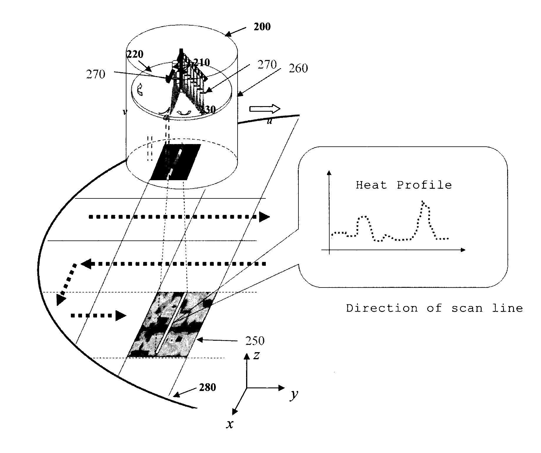
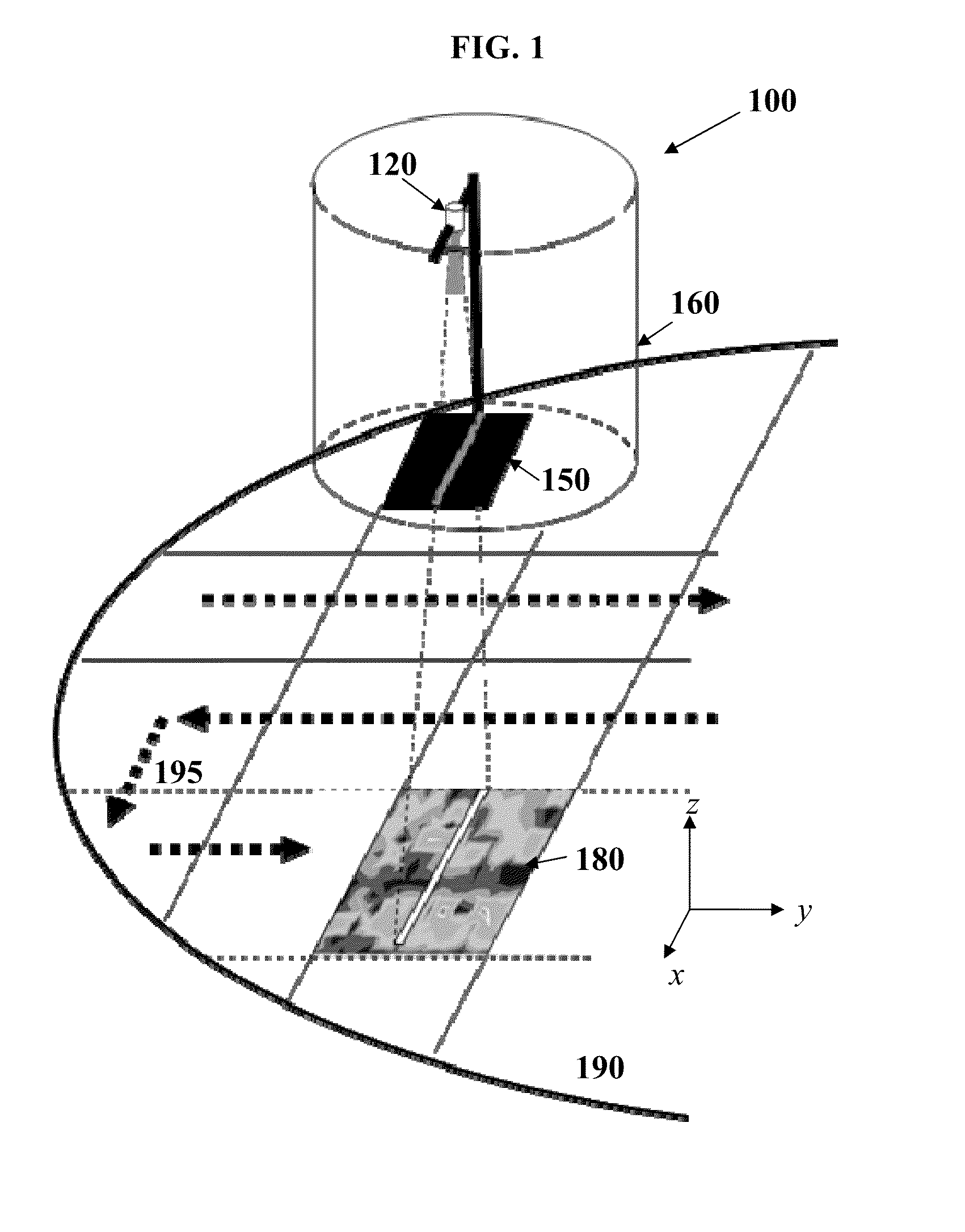
[0036]In each figure, an x-direction represents a direction in which a slit of the mask extends in an annealing device and a y-direction represents a direction in which the annealing device scans the wafer. The x-direction and the y-direction are perpendicular to each other. In the case when the laser device need to change direction at the boundary of the wafer (as shown by the arrow 195 in FIG. 1), the annealing device can move along the x-direction. A z-direction is a direction perpendicular to the wafer plane.

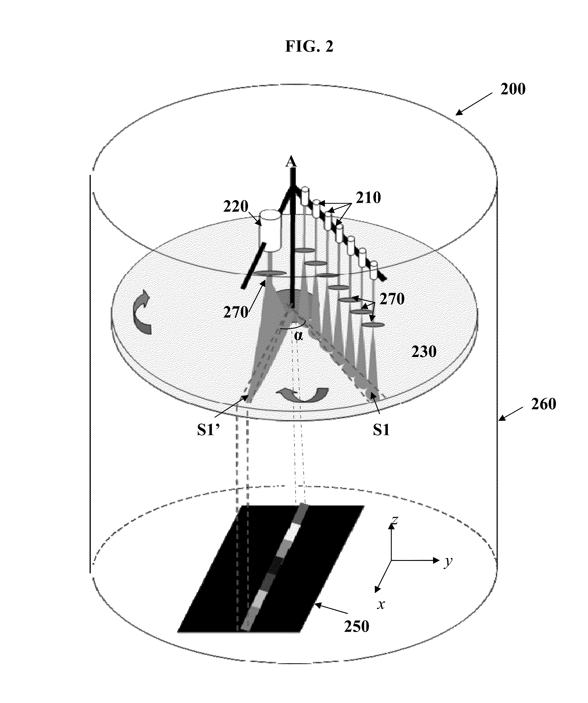
[0037]FIG. 2 shows a laser annealing device 200 according to an embodiment of the present disclosure. The laser annealing device 200 comprises a pump laser source array 210, an annealing laser source 220, and a tunable mask 230. The pump laser source array 210 comprises a plurality of pump laser sources. Each pump laser ...


PUM

PropertyMeasurementUnit
wavelengthaaaaaaaaaa
band gapaaaaaaaaaa
band gapaaaaaaaaaa

Abstract

A laser annealing device for compensating wafer heat maps and its method are disclosed. A laser annealing device comprises a pump laser source array including of a plurality of pump laser sources for irradiating a tunable mask, each pump laser source emitting pump laser, an annealing laser source for emitting annealing laser and irradiating the tunable mask, and a tunable mask for transmitting at least part of the annealing laser after being irradiated by the pump laser.

Description

CROSS-REFERENCE TO RELATED APPLICATIONS[0001]This application claims priority to Chinese Patent Application No. 201210533375.5, filed on Dec. 12, 2012 and entitled “Laser Annealing Device and Method”, which is incorporated herein by reference in its entirety.FIELD OF THE INVENTION[0002]Embodiments of the present invention relate to the field of integrated circuit (IC) fabrication, and more particularly to a laser annealing.DESCRIPTION OF THE RELATED ART[0003]Recently, IC feature size has entered a nanometer era along with the development of semiconductor techniques, and thus new challenges have been raised in IC fabrication. In various techniques set forth to address those challenges, the super shallow junction process for the super shallow junction formation and doping of MOS devices, among others, is practically concerned.[0004]Because annealing in the super shallow junction process requires junction depth as shallow as possible and activation temperature as high as possible, lase...

Claims


Application Information

Patent Timeline
Patent Type & Authority Applications(United States)
IPC IPC(8): H01L21/263
CPCH01L21/268H01L21/324H01L21/02678H01L21/263H01L21/26H01L21/2636B23K26/04B23K26/0736B23K26/0738B23K26/0853G02B27/0922G02B27/0933G02B27/0955G02B27/0977
Inventor CAI, BOXIU
Owner SEMICON MFG INT (SHANGHAI) CORP
Why Eureka
Try Eureka