
Bonding pad of array substrate, method for producing the same, array substrate, and liquid crystal display apparatus

Active Publication Date: 2014-06-19
CHENGDU BOE OPTOELECTRONICS TECH CO LTD +1
View PDF9 Cites 1 Cited by
  • Summary
  • Abstract
  • Description
  • Claims
  • Application Information

AI Technical Summary

Benefits of technology

The present invention provides a new bonding pad structure for an array substrate used in liquid crystal display apparatuses. This structure prevents metal corrosion and improves product quality and stability. The bonding pad includes a first insulation layer, a first conductive layer, a second insulation layer, and a second conductive layer. The second insulation layer has a bonding pad via through which the second conductive layer is electrically connected to the first conductive layer, and the second conductive layer is separated from the S / D layer by the second insulation layer and does not contact with the S / D layer. This avoids water moisture from entering through the second conductive layer and forming a primary battery, preventing metal corrosion in the bonding pad via.

Problems solved by technology

When LCD products are used in various applications, for example, a warm humid condition, a simulation environment experiment, a module assembly, a terminal client user, etc., an unit cell of the LCD product may occur a metallic corrosion in a bonding pad via, causing a line display defect, an abnormal display defect, etc.
Thereby, an electrochemical reaction is taken place and causes the metal material corroded and the LCD product failed.

Method used


Image

  • Bonding pad of array substrate, method for producing the same, array substrate, and liquid crystal display apparatus
  • Bonding pad of array substrate, method for producing the same, array substrate, and liquid crystal display apparatus
  • Bonding pad of array substrate, method for producing the same, array substrate, and liquid crystal display apparatus

Examples


Embodiment Construction

[0044]Exemplary embodiments of the present disclosure will be described hereinafter in detail with reference to the attached drawings, wherein the like reference numerals refer to the like elements. The present disclosure may, however, be embodied in many different forms and should not be construed as being limited to the embodiment set forth herein; rather, these embodiments are provided so that the present disclosure will be thorough and complete, and will fully convey the concept of the disclosure to those skilled in the art.

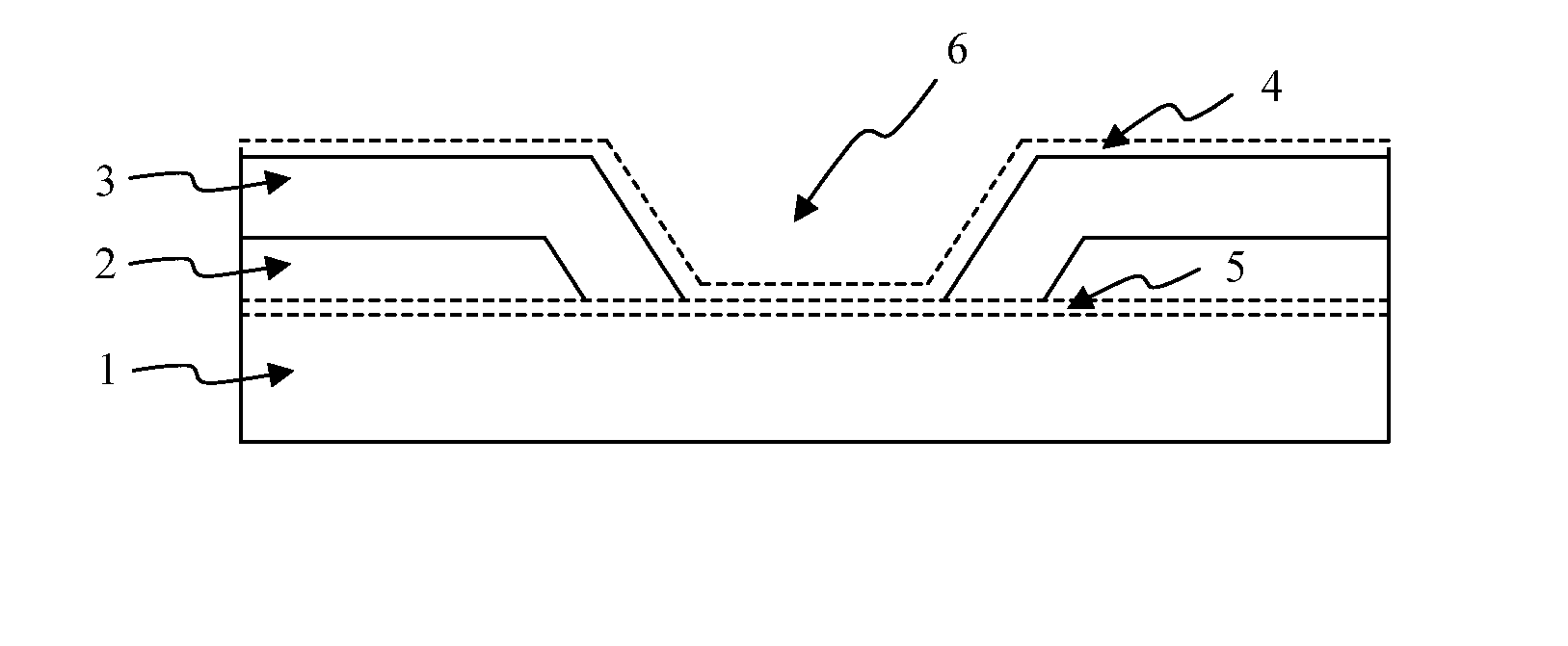
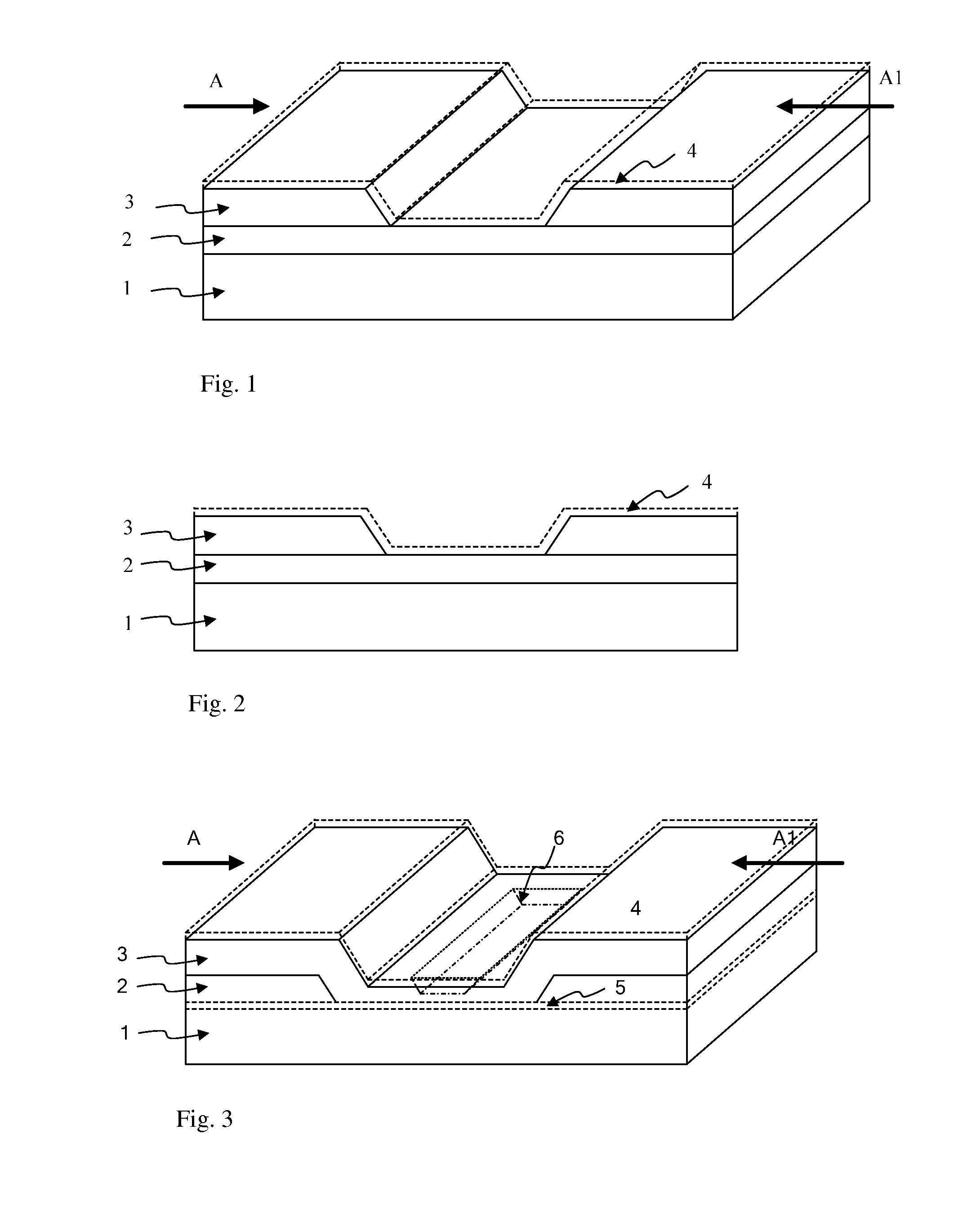
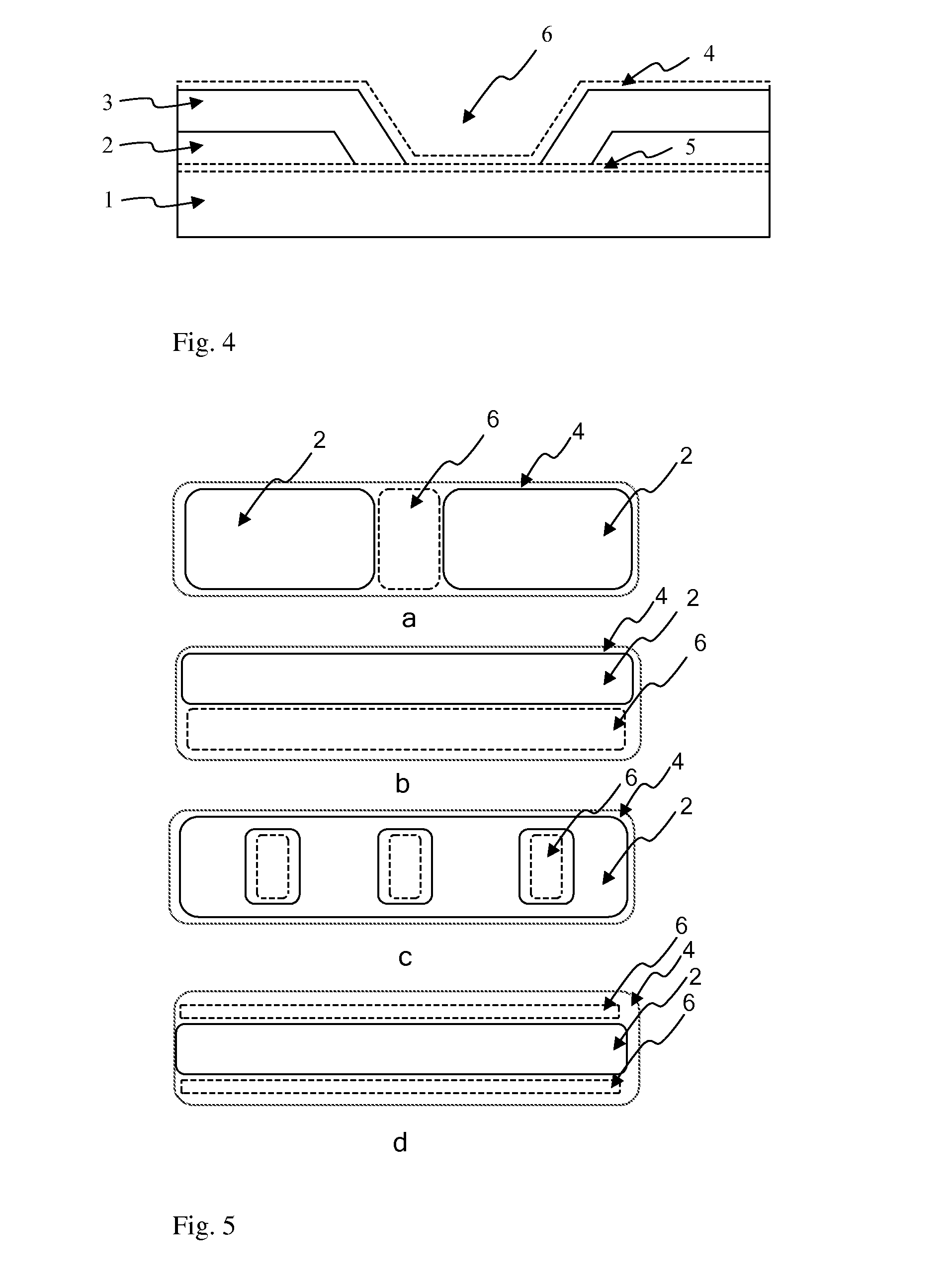
[0045]The general concept of the present invention is to provide a bonding pad of an array substrate, comprising: a gate electrode formed on the array substrate; a first insulation layer formed on the gate electrode; a first conductive layer formed on the first insulation layer; a Source / Drain electrode (S / D) layer formed on the first conductive layer; a second insulation layer formed on the S / D layer; and a second conductive layer formed on the second insula...


PUM


Abstract

A bonding pad of an array substrate, comprising: a gate electrode formed on the array substrate; a first insulation layer formed on the gate electrode; a first conductive layer formed on the first insulation layer; a Source / Drain electrode (S / D) layer formed on the first conductive layer; a second insulation layer formed on the S / D layer; and a second conductive layer formed on the second insulation layer, wherein the second insulation layer is formed with a bonding pad via through which the second conductive layer is electrically connected to the first conductive layer, and the second conductive layer is separated from the S / D layer by the second insulation layer and does not contact the S / D layer. The present invention also discloses a method for producing the bonding pad, an array substrate comprising the bonding pad, and a liquid crystal display apparatus comprising the array substrate.

Description

CROSS-REFERENCE TO RELATED APPLICATION[0001]This application claims the benefit of Chinese Patent Application No. 201210540039.3 filed on Dec. 13, 2012 in the State Intellectual Property Office of China, the whole disclosure of which is incorporated herein by reference.BACKGROUND OF THE INVENTION[0002]1. Field of the Invention[0003]The present invention relates to a manufacturing technology of a liquid crystal display (LCD), more particularly, relates to a bonding pad of an array substrate, a method for producing the same, an array substrate, and a liquid crystal display apparatus.[0004]2. Description of the Related Art[0005]When LCD products are used in various applications, for example, a warm humid condition, a simulation environment experiment, a module assembly, a terminal client user, etc., an unit cell of the LCD product may occur a metallic corrosion in a bonding pad via, causing a line display defect, an abnormal display defect, etc.[0006]By analyzing the metallic corrosion...

Claims


Application Information

Patent Timeline
IPC IPC(8): G02F1/1343H01L21/768H01L23/48
CPCG02F1/1343H01L23/481H01L21/76877H01L21/76816G02F1/13452H01L24/03H01L24/05H01L2924/0002H01L24/00H01L2924/15788H01L2924/00
Inventor LI, QINGSHUO
Owner CHENGDU BOE OPTOELECTRONICS TECH CO LTD
Features
  • Generate Ideas
  • Intellectual Property
  • Life Sciences
  • Materials
  • Tech Scout
  • Unparalleled Data Quality
  • Higher Quality Content
  • 60% Fewer Hallucinations
Learn More