Microlens array, light intensity distribution uniformizing element having same, and projection apparatus having light intensity distribution uniformizing element

a technology of light intensity distribution and microlens array, which is applied in the direction of instruments, planar/plate-like light guides, lenses, etc., can solve the problems of difficult to form the entire surface of the microlenses constituting the microlense array into an ideal lens shape, difficult to form the ideal lens shape around the boundary between adjacent microlenses, and ineffective portions that do not function as desirable lenses

Active Publication Date: 2014-06-19
CASIO COMPUTER CO LTD
View PDF2 Cites 2 Cited by
  • Summary
  • Abstract
  • Description
  • Claims
  • Application Information

AI Technical Summary

Problems solved by technology

In formation of a microlens array with glass, for example, it is difficult to form the entire surfaces of microlenses constituting the microlens array into an ideal lens shape owing to the required processing accuracy.
In particular, it is difficult to form an ideal lens shape around boundaries between adjacent microlenses

Method used


Image

  • Microlens array, light intensity distribution uniformizing element having same, and projection apparatus having light intensity distribution uniformizing element
  • Microlens array, light intensity distribution uniformizing element having same, and projection apparatus having light intensity distribution uniformizing element
  • Microlens array, light intensity distribution uniformizing element having same, and projection apparatus having light intensity distribution uniformizing element

Examples


first embodiment

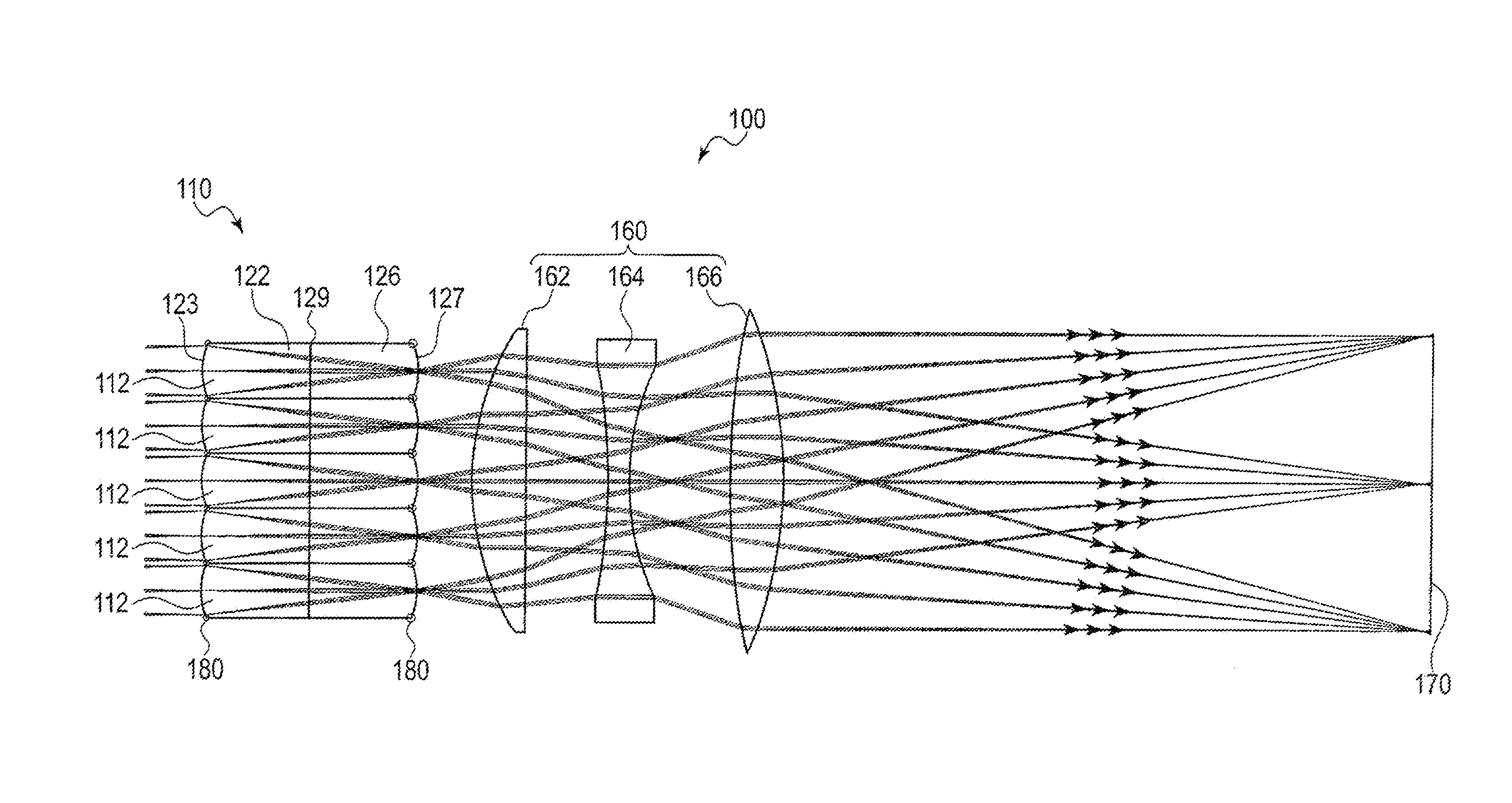
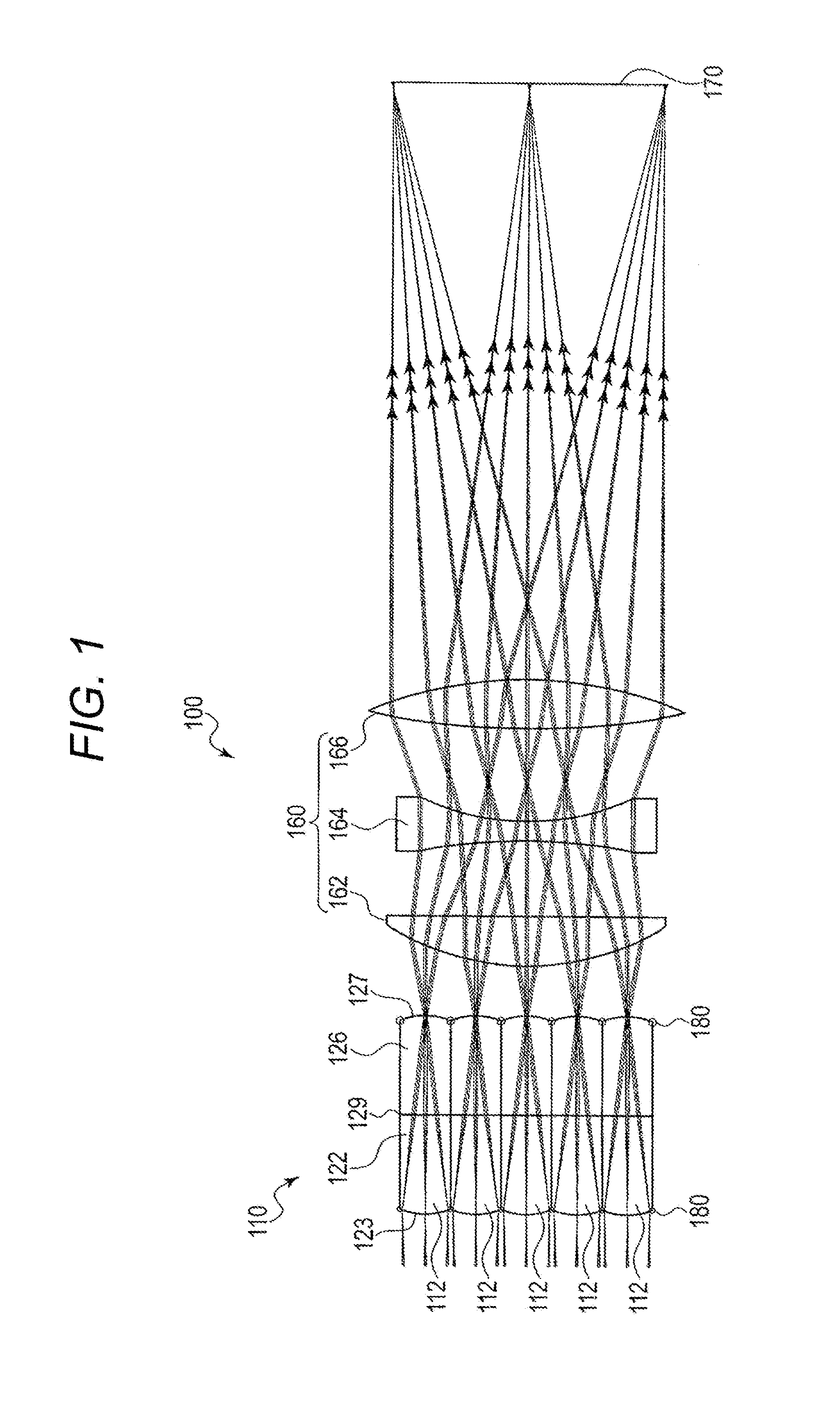
[0019]A first embodiment of the invention will be described with reference to the drawings. FIG. 1 illustrates an outline of an example structure of a light intensity distribution uniformizing element 100 according to the present embodiment. The light intensity distribution uniformizing element 100 includes a microlens array 110 and a coupling lens 160. The coupling lens 160 includes a first lens 162, a second lens 164, and a third lens 166.

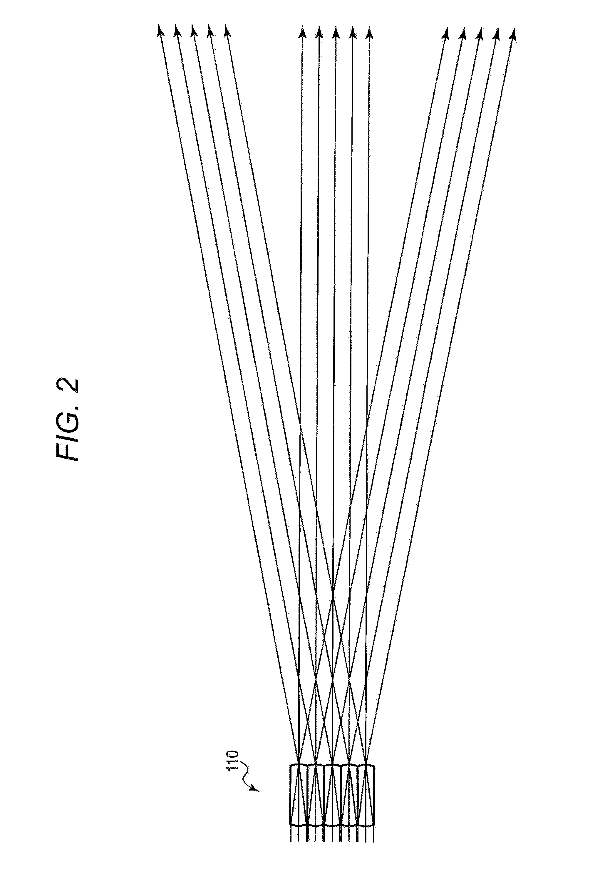
[0020]The microlens array 110 includes multiple microlenses 112. The microlenses 112 are arranged in an array on one plane in a state in which optical axes of the microlenses 112 are parallel. For example, the microlenses 112 are arranged in a rectangular grid pattern.

[0021]The microlens array 110 according to the present embodiment includes a first microlens array 122 provided on the entrance side and a second microlens array 126 provided on the exit side. The first microlens array 122 is made of resin. The second microlens array 126 is made of ...

second embodiment

[0037]A second embodiment will be described with reference to the drawings. The present embodiment is an embodiment of a projection apparatus in which the microlens array according to the first embodiment is used. FIG. 4 illustrates an outline of an example configuration of the projector 10 that is a projection apparatus according to the present embodiment. The projector 10 is a digital light processing (DLP) (registered trademark) projector using a micromirror display device. The projector 10 includes an input unit 11, an image converter 12, a projection processor 13, a micromirror device 14, a light source unit 15, a mirror 16, a projector lens unit 17, a CPU 18, a main memory 19, a program memory 20, an operation unit 21, an audio processor 22, a speaker 23, and a system bus SB.

[0038]The input unit 11 includes terminals such as a pin jack (RCA) type video input terminal and a D-sub 15 type RGB input terminal, and receives analog image signals as input. The input unit 11 converts ...


PUM


Abstract

The present invention provides a microlens array including multiple microlenses arranged axially parallel to one another, wherein entrance surfaces of the microlenses on which light is incident are made of resin, and exit surfaces of the microlenses from which light exits are made of glass.

Description

CROSS-REFERENCE TO RELATED APPLICATIONS[0001]The entire disclosure including the specification, claims, drawings and abstract of Japanese Patent Application No. 2012-276802 filed on Dec. 19, 2012 is incorporated herein by reference.BACKGROUND OF THE INVENTION[0002]1. Field of the Invention[0003]The present invention relates to a microlens array, a light intensity distribution uniformizing element having the same, and a projection apparatus including the light intensity distribution uniformizing element.[0004]2. Description of the Related Art[0005]Microlens arrays in which a large number of microlenses are arranged one-dimensionally or two dimensionally are known. For example, Japanese Patent Application Laid-Open No. 6-250002 discloses a method of manufacturing such microlens arrays. More specifically, a method of manufacturing microlens arrays by using optical patterning and dry etching is disclosed. With the microlenses, a light intensity distribution uniformizing element that uni...

Claims


Application Information

Patent Timeline
IPC IPC(8): G02B3/00G03B21/14
CPCG03B21/142G02B3/005G03B21/208G02B3/00G02B6/003G03B21/14G03B21/602G02B30/27H01L27/14627
Inventor SATO, MAKOTONAKAMURA, HIDEKIOGINO, HIROSHI
Owner CASIO COMPUTER CO LTD
Why Eureka
Try Eureka