

Organic light emitting display device and method of manufacturing the same
a technology of light-emitting display device and organic material, which is applied in the direction of thermoelectric device junction material, semiconductor device, electrical apparatus, etc., can solve the problems of deterioration of viewing angle and efficiency characteristics, and achieve the effect of improving luminous efficiency and color viewing angl
- Summary
- Abstract
- Description
- Claims
- Application Information
AI Technical Summary
Benefits of technology
Problems solved by technology
Method used
Image

Examples
second embodiment
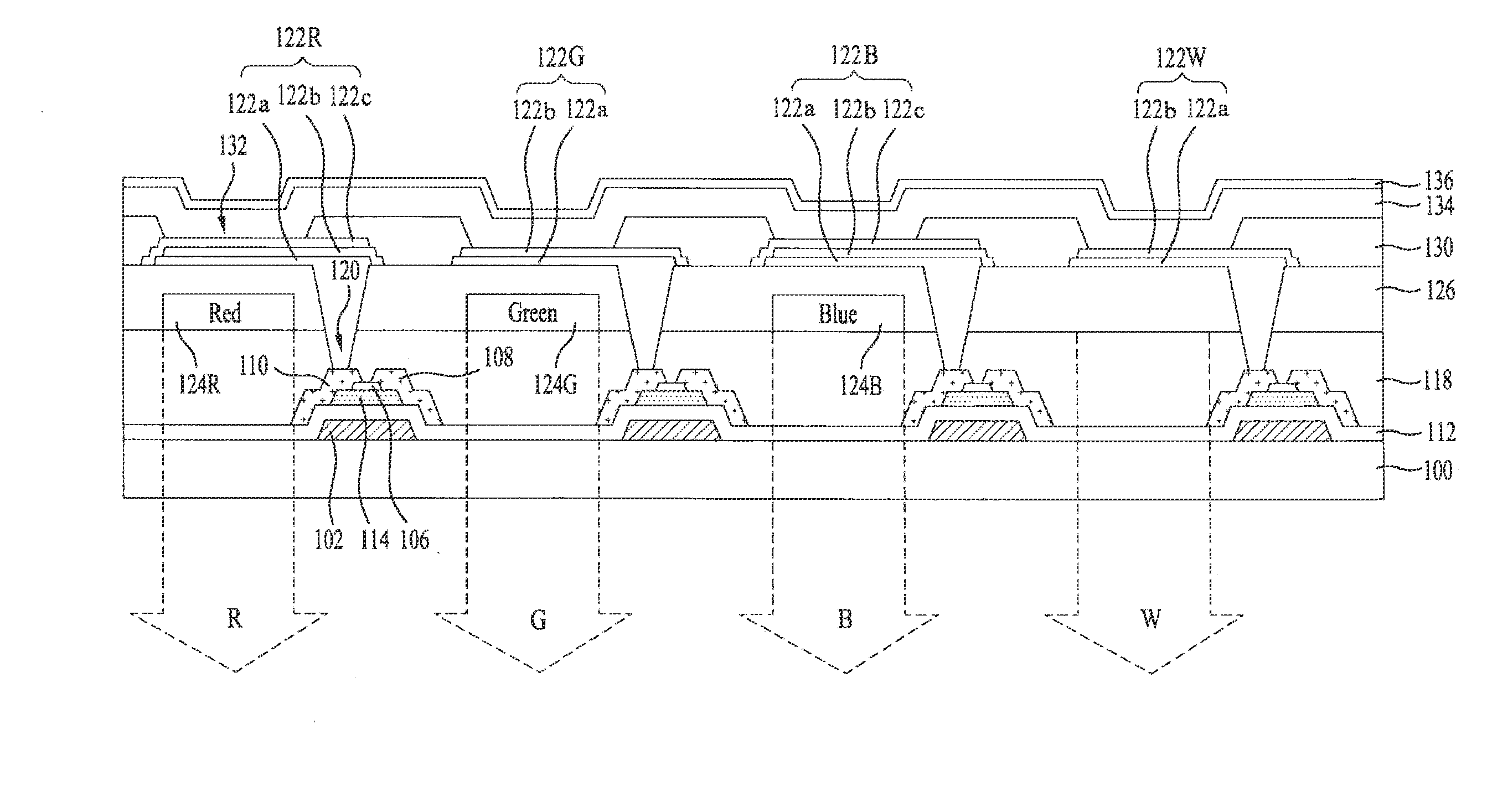
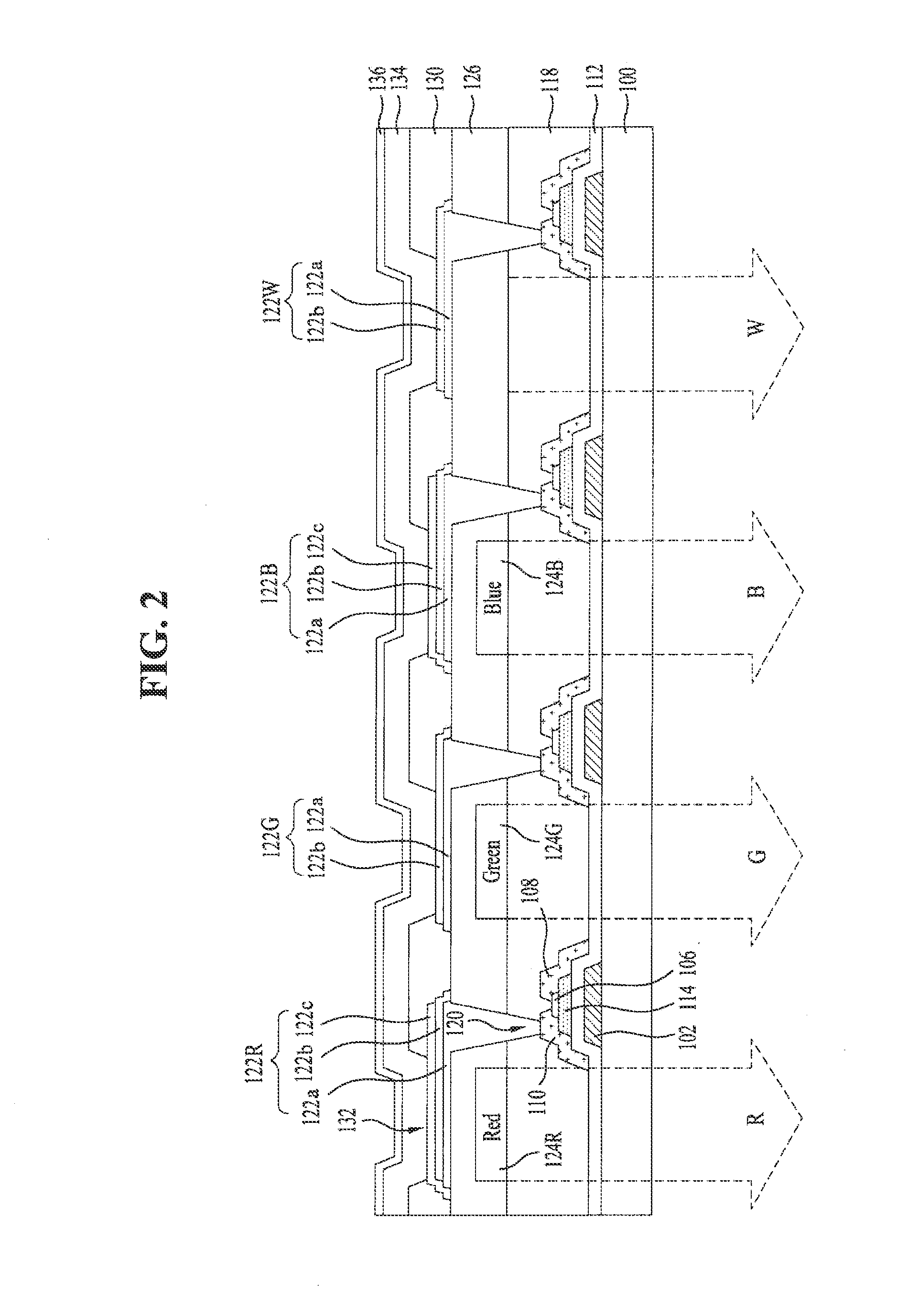
[0086]FIG. 9 is a sectional view of an organic light emitting display device according to the present invention.
[0087]The organic light emitting display device of FIG. 9 includes the same elements as those of the organic light emitting display device of FIG. 1, except that the organic light emitting display device of FIG. 9 includes three light emitting units. Thus, a detailed description of the same elements will be omitted herein.
[0088]The organic common layer 134 of FIG. 9 includes first, second and third light emitting units 134a, 134b and 134c formed between the first and second electrodes 122 and 136, a first charge generation layer CGL1 formed between the first and second light emitting units 134a and 134b, and a second charge generation layer CGL2 formed between the second and third light emitting units 134b and 134c.
[0089]Each of the first, second and third light emitting units 134a, 134b and 134c includes a hole injection layer (HIL), a hole transport layer (HTL), an emis...
third embodiment
[0096]FIG. 11 is a sectional view of an organic light emitting display device according to the present invention.
[0097]The organic light emitting display device of FIG. 11 includes the same elements as those of the organic light emitting display device of FIG. 1, except that the organic light emitting display device of FIG. 11 includes three light emitting units. Thus, a detailed description of the same elements will be omitted herein.
[0098]The organic common layer 134 of FIG. 11 includes the first, second and third light emitting units 134a, 134b and 134c formed between the first and second electrodes 122 and 136, the first charge generation layer CGL1 formed between the first and second light emitting units 134a and 134b, and the second charge generation layer CGL2 formed between the second and third light emitting units 134b and 134c.
[0099]Each of the first, second and third light emitting units 134a, 134b and 134c includes an HIL, an HTL, an EML, and an ETL. In particular, the ...
PUM
 Abstract
Description
Claims
Application Information