Radio frequency amplifier circuit

Active Publication Date: 2014-07-10
PANASONIC SEMICON SOLUTIONS CO LTD
View PDF2 Cites 10 Cited by
  • Summary
  • Abstract
  • Description
  • Claims
  • Application Information

AI Technical Summary

Benefits of technology

[0017]With the radio frequency amplifier circuit according to the present invention, a signal is transmitted between the first distributed constant line and the capacitive element through the lead terminal partially covered with a low-dielectric resin. Further, since the package is mounted on a metallic measurement jig so as to serve as a ground plane, the lead terminal functions as a microstrip line having a low dielectric constant, making it possible to reduce the electrical length from the first distributed constant line to the capacitive element compared with the case of using a high-dielectric material. The

Problems solved by technology

As a result, the input and

Method used


Image

  • Radio frequency amplifier circuit
  • Radio frequency amplifier circuit
  • Radio frequency amplifier circuit

Examples


Example

EMBODIMENT 1

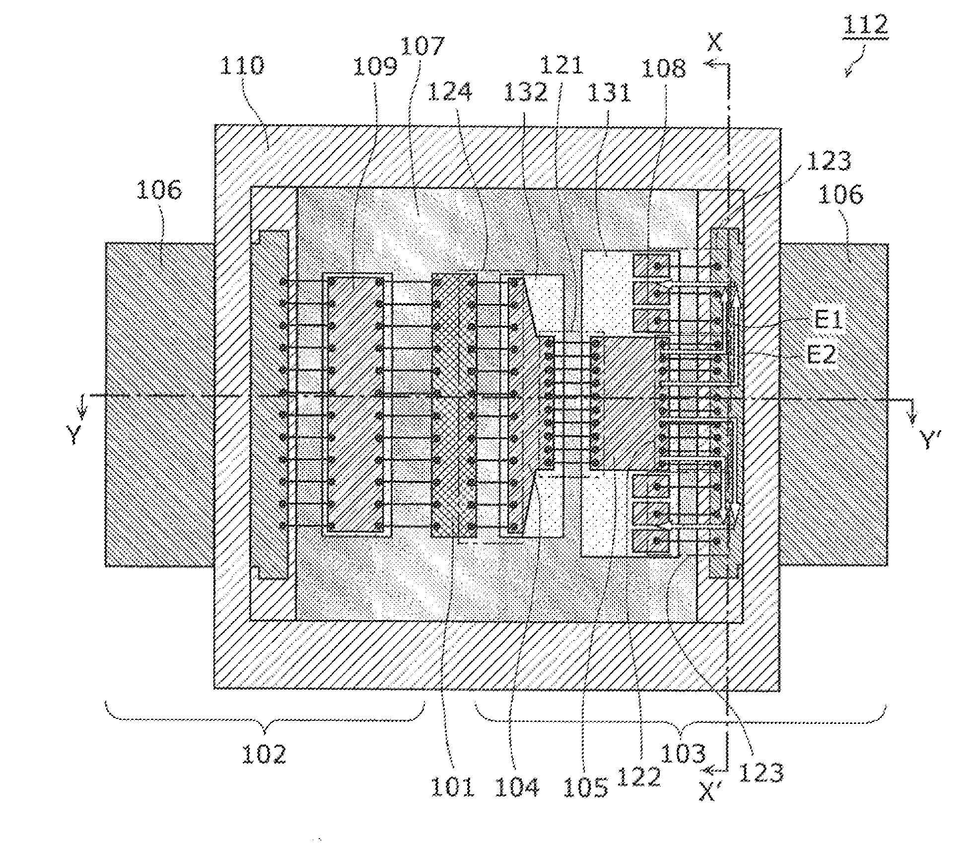
[0054]FIG. 1 illustrates a circuit configuration of a radio frequency amplifier circuit according to Embodiment 1. A radio frequency amplifier circuit 1 according to the present embodiment includes a transistor 101, an input-side matching circuit 102 and an output-side matching circuit 103.

[0055]The transistor 101 has a configuration in which unit transistors are connected in parallel for the purpose of achieving a high power. As a result, the input and output impedances are low. For example, when the output exceeds 100 W, the input and output impedances are sometimes several ohms or lower. Therefore, when the transistor 101 is connected directly to an external circuit normalized to 50Ω, impedance mismatching occurs. In order to resolve this mismatching, the input side and the output side of the transistor 101 are connected to the input-side matching circuit 102 and the output-side matching circuit 103, respectively. The transistor 101 is an amplifier formed of a materia...

Example

EMBODIMENT 2

[0079]FIG. 6 illustrates a layout of a radio frequency amplifier circuit according to Embodiment 2. The radio frequency amplifier circuit according to the present embodiment is constituted by a transistor 101, an input-side matching circuit 102 and an output-side matching circuit 143. The radio frequency amplifier circuit according to the present embodiment is different from the radio frequency amplifier circuit 1 according to Embodiment 1 only in the configuration of the distributed constant line in the output-side matching circuit. The following description will be focused on points different from the radio frequency amplifier circuit 1 according to Embodiment 1.

[0080]The output-side matching circuit 143 includes a first distributed constant line 111, a lead terminal 106 for transmitting a signal to an outside of a package 212 receiving the radio frequency amplifier circuit and a capacitive element 108. An output terminal of the transistor 101 and an input side of the ...

Example

EMBODIMENT 3

[0082]The present embodiment will be directed to a radio frequency amplifier circuit having a matching circuit in which a plurality of unit transmission lines, each having a dielectric distributed constant line and a capacitive element connected in parallel with a lead terminal, are provided in parallel.

[0083]FIG. 7 illustrates a layout of a radio frequency amplifier circuit according to Embodiment 3. The radio frequency amplifier circuit according to the present embodiment is constituted by transistors 101A and 101B, an input-side matching circuit 102 and an output-side matching circuit 153. The radio frequency amplifier circuit according to the present embodiment is different in configuration from the radio frequency amplifier circuit according to Embodiment 2 in that a matching circuit is disposed on an output side of each of a plurality of the transistors. The following description will be focused on points different from the radio frequency amplifier circuit 2 accor...


PUM


Abstract

A radio frequency amplifier circuit includes a transistor and an output-side matching circuit. The output-side matching circuit includes a first distributed constant line to which a radio frequency signal from the transistor is transmitted, a flat plate lead terminal transmitting the radio frequency signal from the first distributed constant line to an outside of the package, and a capacitive element having one electrode that is connected to the lead terminal and the other electrode that is grounded. A back surface of the lead terminal is joined to a resin substrate, and the capacitive element and the first distributed constant line are disposed adjacent to each other, with an alignment direction of the capacitive element and the first distributed constant line intersecting an alignment direction of the first distributed constant line and the lead terminal.

Description

TECHNICAL FIELD [0001]The present invention relates to a radio frequency amplifier circuit and in particular, the configuration of a matching circuit connected to an output side of the radio frequency amplifier circuit.BACKGROUND ART [0002]In general, a radio frequency amplifier circuit has a configuration in which unit transistors are connected in parallel for the purpose of achieving a high power. As a result, the input and output impedances are low. For example, when the output exceeds 100 W, the input and output impedances are sometimes 3Ω or lower. Resulting impedance mismatching with an external circuit normalized to 50Ω to which the radio frequency amplifier circuit is to be connected requires a matching circuit to be connected to an input side and an output side of the radio frequency amplifier circuit.[0003]The matching circuit for matching the low impedance of the nearly short-circuited radio frequency amplifier circuit to 50Ω is configured, for example, by the combination...

Claims


Application Information

Patent Timeline
IPC IPC(8): H03F1/56
CPCH01L23/66H01L2223/6655H01L2224/48091H01L2224/48137H01L2224/49175H03F3/601H01L2224/73265H03F1/565H03F1/56H01L2924/00014H01L2223/6611H01L2924/3011H01L2924/30111H03F3/191H01L2924/00
Inventor KAMIYAMA, TOMOHIDENAITOU, HIROSHIUNO, TAKASHIIWATA, MOTOYOSHIYAHATA, KAZUHIROIKEDA, HIKARU
Owner PANASONIC SEMICON SOLUTIONS CO LTD
Why Eureka
Try Eureka