Amplification Method For Photoresist Exposure In Semiconductor Chip Manufacturing

a technology of photoresist and semiconductor chip, which is applied in the field of exposing an extreme ultraviolet (euv) photoresist, can solve the problems of insufficient euv lithography to achieve the required utilization performance, feature edge roughness, and minimum feature size resolution, so as to reduce image blurring, improve image resolution, and reduce lateral diffusion

Inactive Publication Date: 2014-07-10
IBM CORP
View PDF2 Cites 13 Cited by
  • Summary
  • Abstract
  • Description
  • Claims
  • Application Information

AI Technical Summary

Benefits of technology

[0005]An electrical field is applied through an extreme ultraviolet (EUV) photoresist layer along a direction perpendicular to an interface between the EUV photoresist layer and an underlying layer. Secondary electrons and thermal electrons are accelerated along the direction of the electrical field, and travel with directionality before interacting with the photoresist material for a chemical reaction. The directionality reduces lateral diffusion of the secondary an

Problems solved by technology

Currently, the imaged feature edge roughness, as well as resolution of the minimum feature size, is insufficient

Method used


Image

  • Amplification Method For Photoresist Exposure In Semiconductor Chip Manufacturing
  • Amplification Method For Photoresist Exposure In Semiconductor Chip Manufacturing
  • Amplification Method For Photoresist Exposure In Semiconductor Chip Manufacturing

Examples


Embodiment Construction

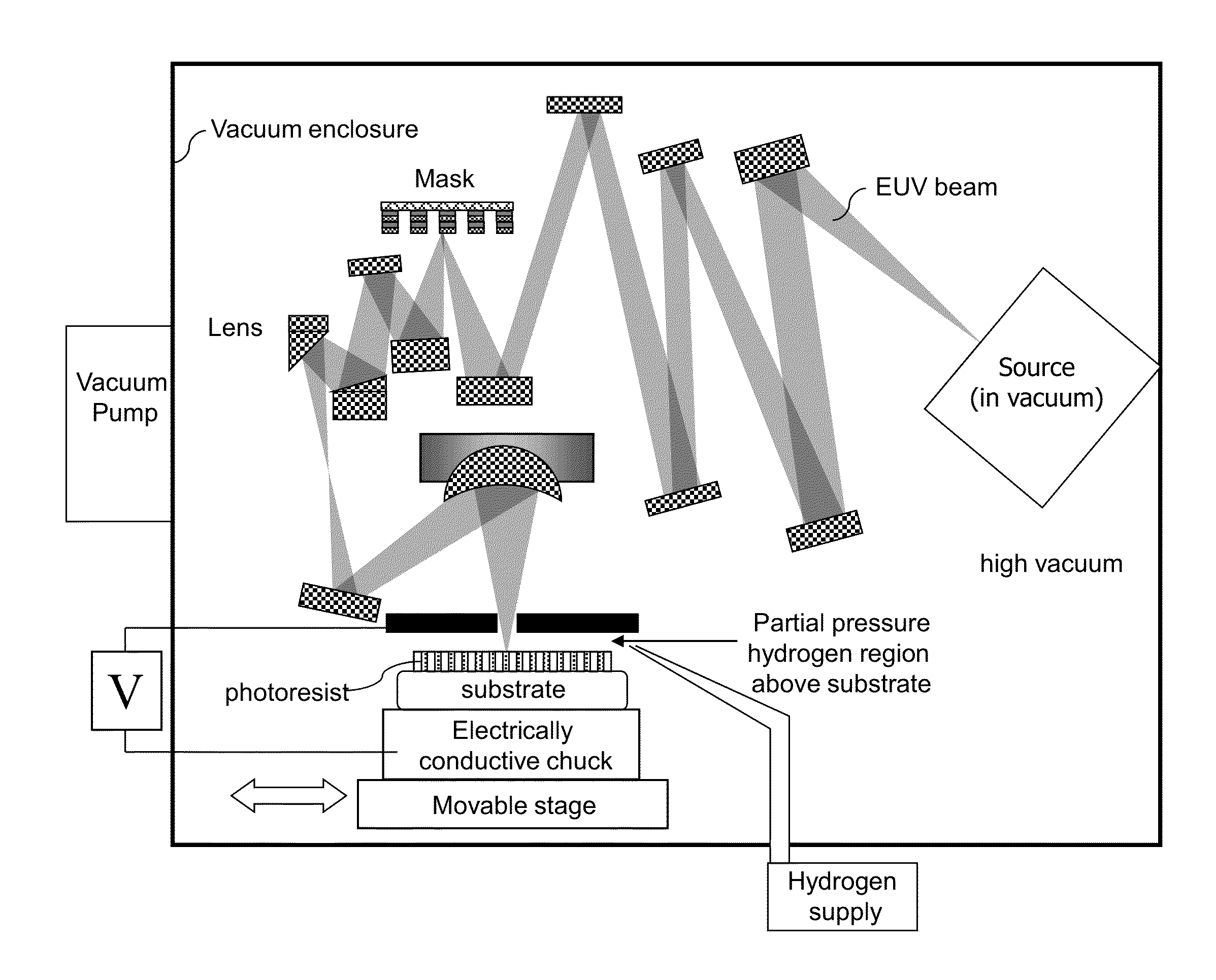
[0011]As stated above, the present disclosure relates to a method of exposing an extreme ultraviolet (EUV) photoresist, and an apparatus for implementing the same. Aspects of the present disclosure are now described in detail with accompanying figures. Throughout the drawings, the same reference numerals or letters are used to designate like or equivalent elements. The drawings are not necessarily drawn to scale.

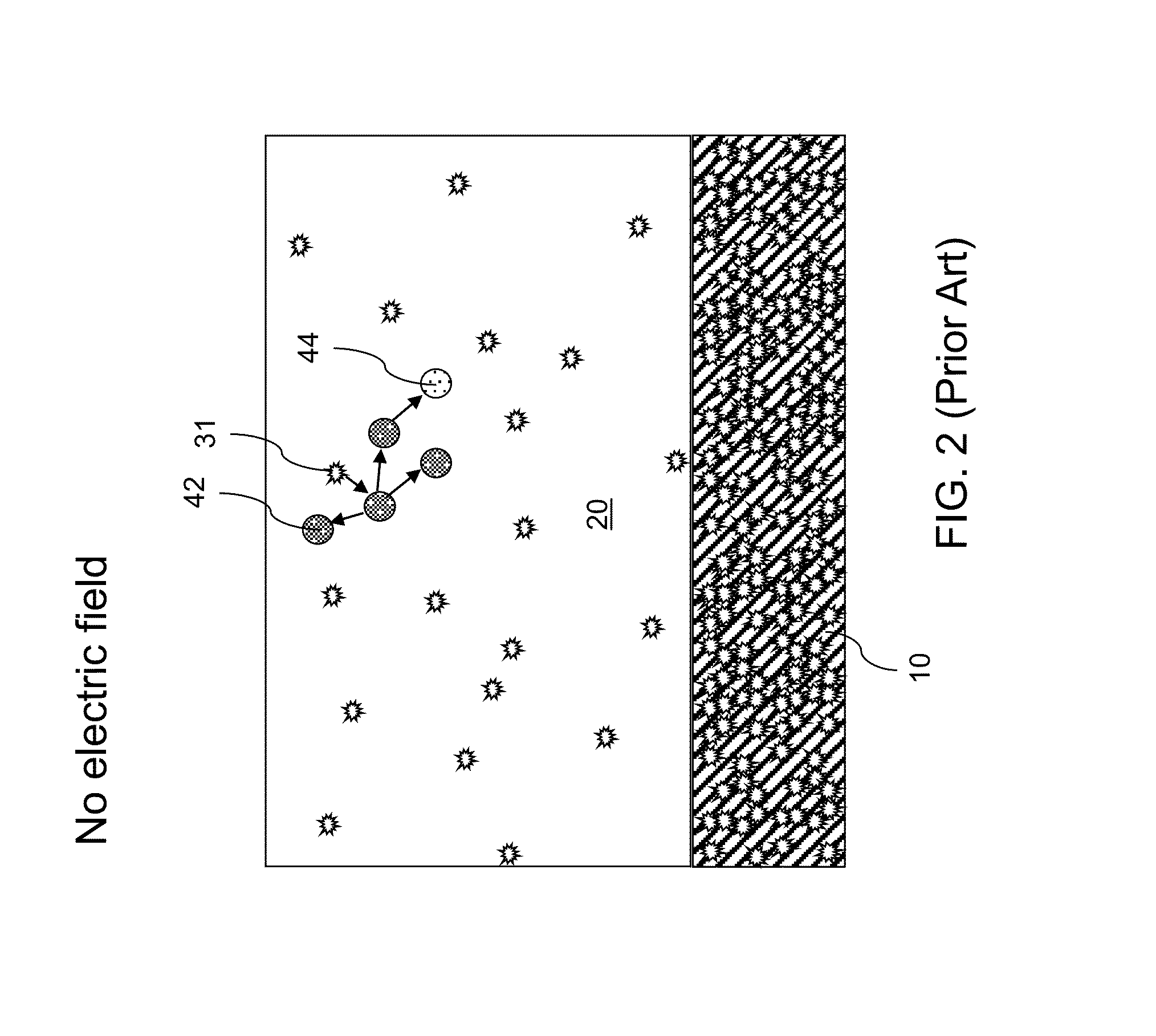
[0012]During conventional extreme ultraviolet (EUV) lithography, a majority of secondary electrons is lost in non-imaging layers due to poor absorption in an imaging layer, i.e., the EUV photoresist layer. The loss of the secondary electrons in the non-imaging layers is responsible for the requirement for a high exposure dose in conventional EUV lithography tools.

[0013]According to an embodiment of the present disclosure, a direct current (DC) electrical bias, an alternating current (AC) electrical bias, or a combination of a DC electrical bias and an AC electrical bias is a...


PUM


Abstract

An electrical field is applied through an extreme ultraviolet (EUV) photoresist layer along a direction perpendicular to an interface between the EUV photoresist layer and an underlying layer. Secondary electrons and thermal electrons are accelerated along the direction of the electrical field, and travel with directionality before interacting with the photoresist material for a chemical reaction. The directionality increases the efficiency of electron photoacid capture, reducing the required EUV dose for exposure. Furthermore, this directionality reduces lateral diffusion of the secondary and thermal electrons, and thereby reduces blurring of the image and improves the image resolution of feature edges formed in the EUV photoresist layer. The electrical field may be generated by applying a direct current (DC) and/or alternating current (AC) bias voltage across an electrostatic chuck and a conductive plate placed over the EUV photoresist layer with a hole for passing the EUV radiation through.

Description

BACKGROUND[0001]The present disclosure relates to a method of exposing an extreme ultraviolet (EUV) photoresist, and an apparatus for implementing the same.[0002]Extreme ultraviolet lithography is a lithography technology using an extreme ultraviolet (EUV) wavelength radiation for exposure. As used herein, EUV refers to a range of electromagnetic radiation having a wavelength from 10 nm to 50 nm. When an EUV photon is absorbed in a photoresist, at least one photoelectron, secondary electrons, and thermal electrons are generated by ionization. The photoelectrons are generated as a direct result of a photon-matter interaction between the EUV photon and the matter in the photoresist layer. The secondary electrons are caused by collision of the photoelectron with additional electrons as the photoelectron travels through the photoresist material. The thermal electrons are derived from the photoelectrons or the secondary electrons due to their energy loss or due to collisions that transfe...

Claims


Application Information

Patent Timeline
IPC IPC(8): G03F7/20
CPCG03F7/2004G03F7/70308G03F7/70325G03F7/70375G03F7/2041G03F7/70058
Inventor WISE, RICHARD S.CORLISS, DANIEL A.
Owner IBM CORP
Why Eureka
Try Eureka