ESD protection circuit

a protection circuit and circuit technology, applied in the direction of semiconductor devices, semiconductor/solid-state device details, electrical apparatus, etc., to achieve the effect of discharging an esd current and saving layout area

Active Publication Date: 2014-07-17
MACRONIX INT CO LTD
View PDF0 Cites 16 Cited by
  • Summary
  • Abstract
  • Description
  • Claims
  • Application Information

AI Technical Summary

Benefits of technology

[0006]The objective of the present invention is to provide an ESD protection circuit. In the ESD protection circuit, a well with a different conductivity type to the substrate in which it embeds, is added to surround a snapback device for dissipating an ESD current. Additionally, a doped region is formed in the well to be electrically coupled to a voltage pad susceptible ...

Problems solved by technology

Additionally, a doped region is formed in the well to be electrically coupled to a voltage ...

Method used


Image

  • ESD protection circuit
  • ESD protection circuit
  • ESD protection circuit

Examples


Embodiment Construction

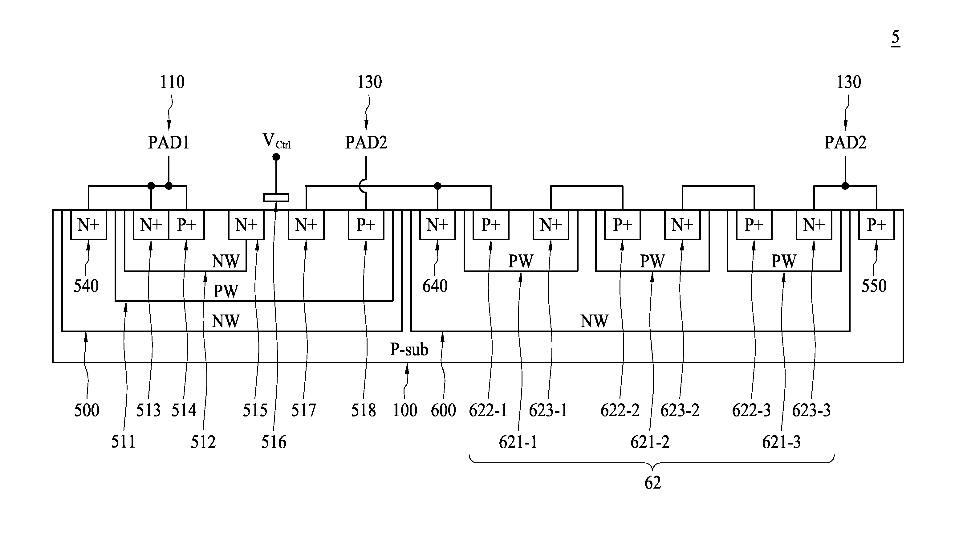
[0026]The embodiments of the present invention are described more fully hereinafter with reference to the accompanying drawings, which form a part hereof, and which show, by way of illustration, specific exemplary embodiments by which the invention may be practiced. This invention may, however, be embodied in many different forms and should not be construed as limited to the embodiments set forth herein; rather, these embodiments are provided so that this disclosure will be thorough and complete, and will fully convey the scope of the invention to those skilled in the art. As used herein, the term “or” is an inclusive “or” operator, and is equivalent to the term “and / or,” unless the context clearly dictates otherwise. In addition, throughout the specification, the meaning of “a,”“an,” and “the” include plural references. The term “coupled” implies that the elements may be directly connected together or may be coupled through one or more intervening elements.

[0027]FIG. 3 is an equiva...


PUM


Abstract

An electrostatic discharge (ESD) protection circuit is coupled between first and second pads to protect an internal circuit therebetween. Under a normal operating condition, a voltage on the first pad is higher than that on the second pad. The ESD protection circuit includes a substrate of a first conductivity type; first well of a second conductivity type in the substrate, wherein the first well is coupled to the first pad; a snapback device housed in the first well; and a diode string in the substrate, connected in series with the snapback device and separated from the first well, wherein the serially connected diode string and snapback device is connected between the first pad and the second pad. With the isolation from the first well, the holding voltage of the ESD protection circuit can be tuned by adjusting the number of diodes in the diode string without using a guard ring.

Description

FIELD OF THE INVENTION[0001]The present invention relates in general to an ESD protection circuit, and more particularly to an ESD protection circuit with a tunable holding voltage.BACKGROUND[0002]Protecting an internal circuit from the threat of ESD damage has been an ongoing challenge for those skilled in the art. Snapback devices are a well-known class of devices that are being adopted in ESD protection circuits. Devices of such a class exhibit a snapback behavior when ESD overstress occurs. FIG. 1 is a diagram showing an I-V curve of a snapback device with a snapback behavior. As illustrated in FIG. 1, when a voltage across the snapback device is below a trigger voltage Vtrig, the snapback device remains cutoff. When the voltage reaches the trigger voltage Vtrig, a p-n junction of the snapback device enters a condition of an avalanche breakdown and triggers a parasitic BJT transistor of the snapback device to turn on and starts conducting a current. Once the snapback device star...

Claims


Application Information

Patent Timeline
IPC IPC(8): H01L27/08H01L23/552H01L27/088
CPCH01L27/08H01L27/088H01L23/552H01L27/0248Y10S257/91
Inventor HE, CHIEH WEIXU, QI ANYU, JUN JUNHAO, HAN
Owner MACRONIX INT CO LTD
Why Eureka
Try Eureka