
Dielectric structures in solar cells

a solar cell and dielectric structure technology, applied in the field of device fabrication, can solve the problems of limiting the generation of carriers in the cell, higher cost per watt of power generated than the less efficient commercially produced screen-printed silicon solar cell, and higher manufacturing cos

Inactive Publication Date: 2014-07-17
NEWSOUTH INNOVATIONS PTY LTD
View PDF10 Cites 21 Cited by
  • Summary
  • Abstract
  • Description
  • Claims
  • Application Information

AI Technical Summary

Benefits of technology

The patent describes a method for creating a layer of material over a porous layer, which can seal the pores or extend into them. The technical effect of this method is the ability to create a layer of material that can trap air or extend into the pores of the porous layer.

Problems solved by technology

One of the limitations of screen printed solar cells is that screen printed metal fingers formed on the illuminated surface of the solar cell effectively shade the cell and thus limit the generation of carriers in the cell.
Such rear contact cells have been successfully manufactured, however although efficiencies as high as 24% have been achieved in a production environment, these rear contact technologies typically result in a higher cost per Watt of power generated than the less efficient commercially-produced screen-printed silicon solar cells.
The higher cost of manufacture arises from the more complex processing required and the need to use higher quality silicon wafers to ensure that carriers generated towards the front (illuminated) surface of the solar cell can travel to a rear junction to be collected by the metal contacts.

Method used


Image

  • Dielectric structures in solar cells
  • Dielectric structures in solar cells
  • Dielectric structures in solar cells

Examples


Embodiment Construction

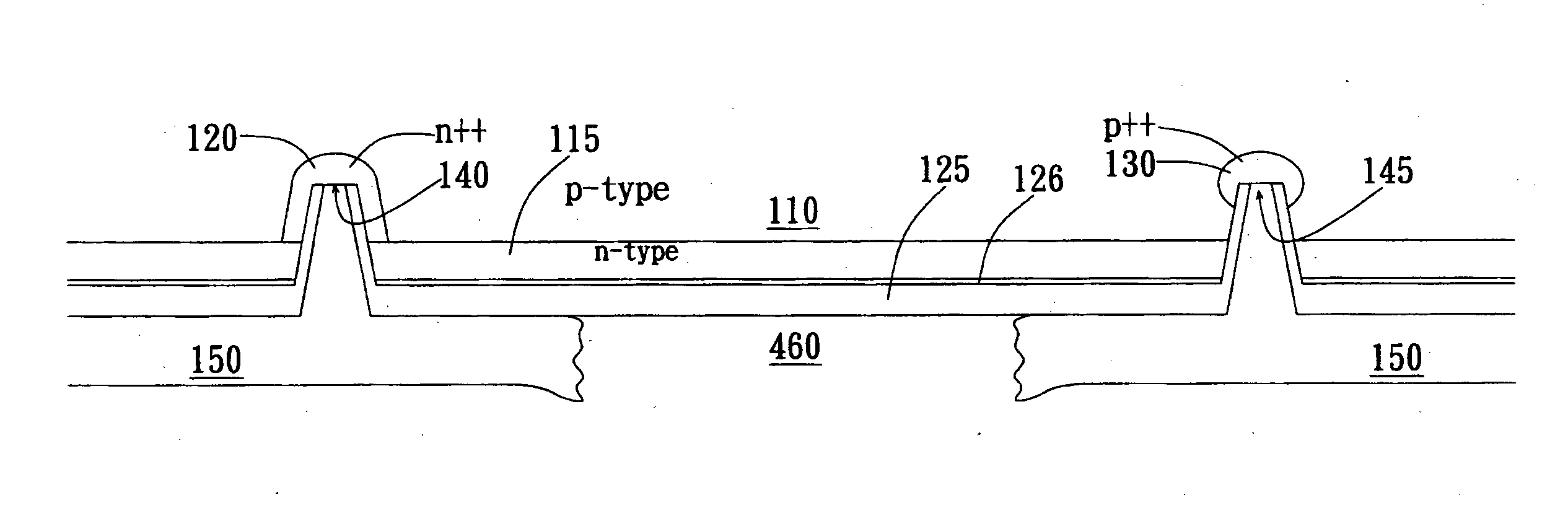
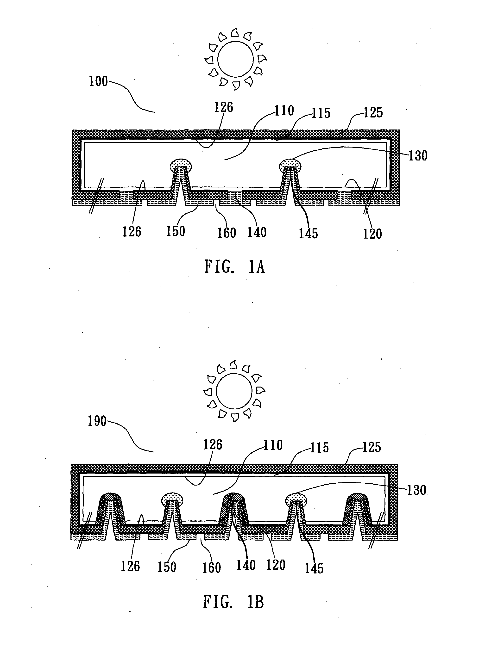
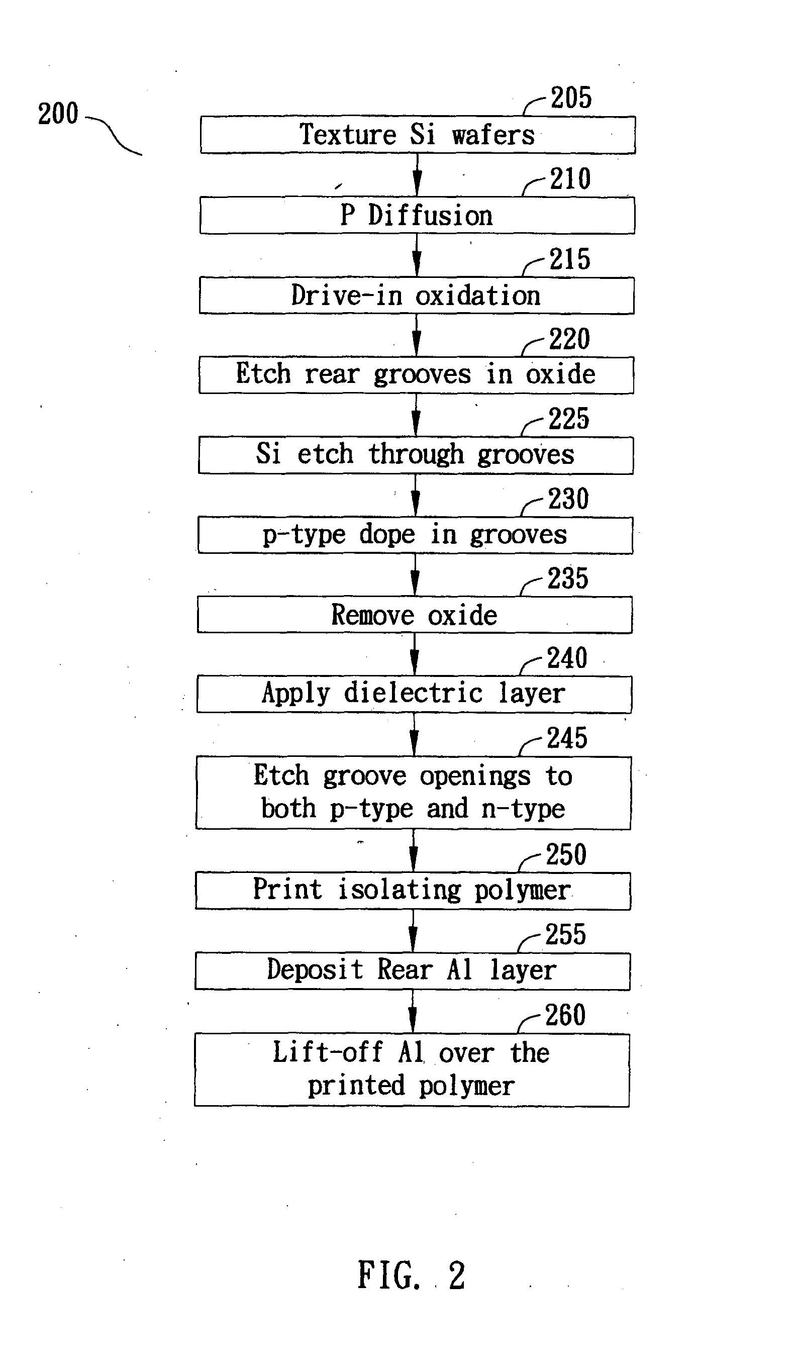
[0081]Fabrication of low-cost solar cell devices requires processes which can minimise material usage and / or utilise, where possible, less expensive materials. For screen-printed solar cells, the cost of silicon wafers will continue to dominate the cost of devices even though large cost savings have been made in cell conversion costs over the past 5-10 years. Processes which can enable the use of thinner wafers can significantly reduce the cost of final devices. Furthermore, thinner wafers, if well passivated, can result in higher energy conversion efficiencies due to a reduction in the dark saturation current. The process of screen printing can result in high breakage rates as the wafer thickness reduces to values of ˜160 μm and therefore this presents a limit to how thin wafers can ultimately be for the currently dominant patterning and metallisation process. If further gains are to be made with respect to using even thinner silicon substrates then alternative methods of patternin...


PUM

PropertyMeasurementUnit
temperaturesaaaaaaaaaa
thicknessaaaaaaaaaa
thickaaaaaaaaaa

Abstract

A dielectric, structure and a method of forming a dielectric structure for a rear surface of a silicon solar cell are provided. The method comprises forming a first dielectric layer over the rear surface of the silicon solar cell, and then depositing a layer of metal such as aluminum over the first dielectric layer. The metal layer is then anodized to form a porous layer and a material layer is deposited over a surface of the porous layer such that the material deposits on the surface of the porous layer without contacting the silicon surface.

Description

COPYRIGHT NOTICE[0001]A portion of the disclosure of this patent document contains material that is subject to copyright protection. The copyright owner has no objection to the facsimile reproduction by anyone of the patent document or the patent disclosure, as it appears in the Patent and Trademark Office patent files or records, but otherwise reserves all copyright rights whatsoever.TECHNICAL FIELD OF THE INVENTION[0002]The present invention relates generally to the field of device fabrication and, in particular, to the formation of a structure that assists light trapping in solar cells.BACKGROUND OF THE INVENTION[0003]The fabrication of solar cell semiconductor devices typically involves the formation of metal contacts to a p-n junction device. The semiconductor material (e.g., silicon) absorbs light and generates electron and hole carriers which can then be separated by the p-n junction in the device. Majority carriers (e.g., electrons in n-type semiconductor material) are colle...

Claims


Application Information

Patent Timeline
Patent Type & Authority Applications(United States)
IPC IPC(8): H01L31/0224
CPCH01L31/022441H01L21/2254H01L31/02168H01L31/056H01L31/0682H01L31/1868H01L31/188Y02E10/52Y02E10/547Y02P70/50
Inventor LENNON, ALISON JOANLI, ZHONGTIANWENHAM, STUART ROSSLU, PEI HSUAN
Owner NEWSOUTH INNOVATIONS PTY LTD
Features
  • Generate Ideas
  • Intellectual Property
  • Life Sciences
  • Materials
  • Tech Scout
  • Unparalleled Data Quality
  • Higher Quality Content
  • 60% Fewer Hallucinations
Learn More