System and Device for Non-Destructive Raman Analysis

Active Publication Date: 2014-07-24
HOLOGIC INC
View PDF0 Cites 5 Cited by
  • Summary
  • Abstract
  • Description
  • Claims
  • Application Information

AI Technical Summary

Benefits of technology

[0010]According to one aspect of the invention, an extender for extending an optical reach of a microspectrometer includes a housing including a proximal orifice, a distal orifice and a mounting plate for attaching the housing to a microscope of the microspectrometer such that a lens of the microscope is aligned with the proximal orifice. A plurality of minors is positioned within the housing to provide an optical channel between the proximal orifice and the distal orifice of the housing to thereby extend the optical reach of the microspectrometer. The addition of the extender to the microspectrometer thus enables oversized samples to be analyzed, repaired and returned to production without destruction.
[0011]According to another aspect of the invention, a supplemental stage for use with a microspectrometer having an existing stage is provided. The supplemental stage includes a tray for supporting an oversized sample and a motorized travel system for controlling a travel movement of the tray in at least one of an x and y direction, wherein the oversized sample exceeds the travel capabilities of the existing stage in at least one of the x and y directions, and wherein the travel capabilities of the motorized travel system are at least matched to the x and y dimensions of the oversized sample. In addition, a controller couples a stage controller of the microspectrometer to the motorized travel system. With such an arrangement, software tools of the microspectrometer may eas

Problems solved by technology

However it is sometimes desirable to perform Raman analysis on samples having a size that exceeds that of an existing optical microscope stage.
However anomalies in the manufacturing process may give rise to defects within the amorphous selenium that impair the free movement of electron hole pairs.
For example, temperature changes or other processing procedures may cause crystals to be generated in the selenium.
However it is difficult to use existing Raman microspectrometers to analyze digital image panels in their entirety becau

Method used


Image

  • System and Device for Non-Destructive Raman Analysis
  • System and Device for Non-Destructive Raman Analysis
  • System and Device for Non-Destructive Raman Analysis

Examples


example

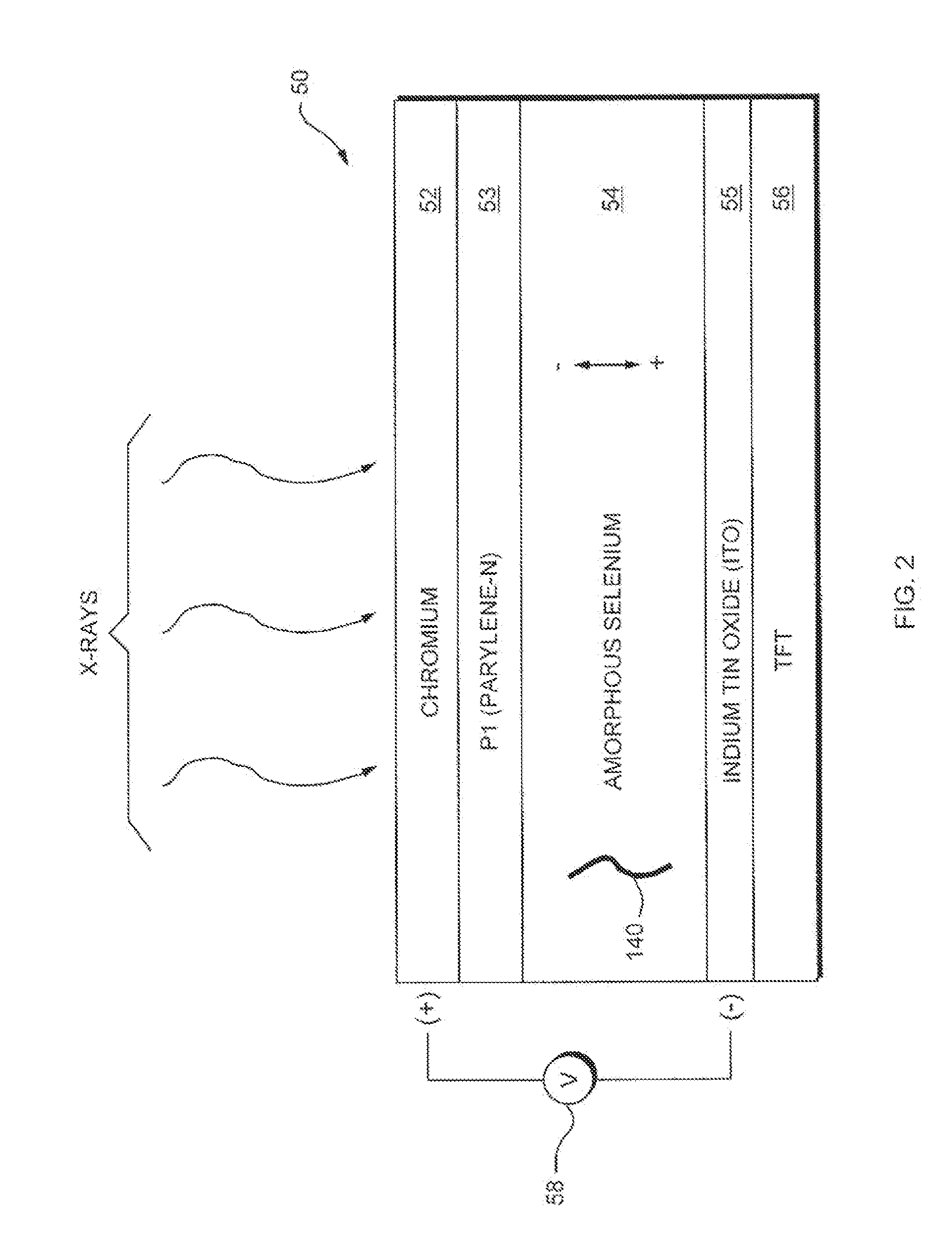
[0054]This example describes sensitivity of a Raman microspectrometer for crystallized selenium in a mammography panel generally composed of amorphous selenium.

[0055]Sensitivity is compared between a Raman microspectrometer with an optical extension and a Raman microspectrometer without an optical extension.

TABLE 1Conditions for Testing Sensitivity of a Raman Microspectrometer forPresence of Crystallized Selenium in an Otherwise Amorpohous SeleniumMammography PanelWith An Optical Extension(Length = 539 mm;Mirror-to-Mirror Length = 454 mm;Raman MicrospectrometerWidth = 62 mm;ParameterHeight = 50 mm)Without An Optical ExtensionSpectrometerAlmega XRAlmega XRLaser780 nm780 nmLaser Power Level3.5 mW (10% of 35 mW)3.5 mW (10% of 35 mW)Laser PolarizationparallelparallelCosmic Ray ThresholdlowlowGrating360 lines / mm360 lines / mmSpectrograph Aperture for(1) 25 μm pinhole and (2) 100 μm(1) 25 μm pinhole and (2) 100 μmConfocalitypinholepinholeSample PositionmicroscopemicroscopeCCD Camera Tempera...


PUM


Abstract

A Raman microspectrometer system extends the optical reach and analysis range of an existing Raman microspectrometer to allow analysis and/or repair of an oversized sample. The Raman microspectrometer system includes an extender for extending the optical reach of the existing microspectrometer and a supplemental stage which extends the analysis range of the existing microspectrometer by providing travel capabilities for non-destructive analysis of an entire oversized sample. Such an arrangement decreases manufacturing costs associated with testing oversized samples such as mammography panels, enabling analysis and/or repair to be performed without destruction.

Description

CROSS-REFERENCE TO RELATED APPLICATIONS[0001]This application is a continuation-in-part and claims priority under 35 U.S.C. §120 to U.S. patent application Ser. No. 13 / 541,883, filed Jul. 5, 2012, which is a divisional of U.S. patent application Ser. No. 12 / 179,251, filed Jul. 24, 2008. Each of the above applications is hereby incorporated by reference.FIELD OF THE INVENTION[0002]This invention relates generally to the field of micro-spectrometry and more particularly to a non-destructive method and apparatus for identifying, analyzing and repairing digital imaging panels using a microspectrometer.BACKGROUND OF THE INVENTION[0003]FIG. 1 illustrates a typical Raman microspectrometer 10. The Raman microspectrometer 10 includes an optical microscope 20, coupled via supports 32 and 34 to a combined excitation laser source / spectrometer 30. The Raman microspectrometer is used to analyze the molecular structure of a sample that is disposed on the microscope stage 22. During analysis the sa...

Claims


Application Information

Patent Timeline
IPC IPC(8): G01J3/44G01J3/02
CPCG01J3/0218G01J3/0256G01J3/44G01N21/95G01J3/02G01J3/021G01J3/0291G01J3/4412G02B21/24G01J3/0208G01J3/0202G01J3/027G01N21/65
Inventor MAZZIO, VICTOR
Owner HOLOGIC INC
Why Eureka
Try Eureka