Leadframe-Based Semiconductor Package Having Terminals on Top and Bottom Surfaces

a technology of semiconductor packages and terminals, applied in semiconductor devices, semiconductor/solid-state device details, electrical apparatus, etc., can solve problems such as fracture failures and significant thermo-mechanical stresses, and achieve the effect of avoiding parasitic interconnection losses, electronic noise, and waste of valuable board real esta

Inactive Publication Date: 2014-07-31
TEXAS INSTR INC
View PDF2 Cites 23 Cited by
  • Summary
  • Abstract
  • Description
  • Claims
  • Application Information

AI Technical Summary

Benefits of technology

[0012]It is a technical advantage of the invention that the method can fabricate devices with cantilever leads protruding from the package, which can accommodate, under a force lying in the plane of the expanding and contracting substrate, elastic bending and stretching beyond the limit of simple elongation based upon inherent lead material characteristics. Such elastic cantilever properties can be achieved by cantilever geometries, which ma

Problems solved by technology

When an industrial application of a PoP assembled on a board involves wide and abrupt temperature swings, significant thermo-mechanical stresses are caused due to widely different coefficients o

Method used


Image

  • Leadframe-Based Semiconductor Package Having Terminals on Top and Bottom Surfaces
  • Leadframe-Based Semiconductor Package Having Terminals on Top and Bottom Surfaces
  • Leadframe-Based Semiconductor Package Having Terminals on Top and Bottom Surfaces

Examples


Embodiment Construction

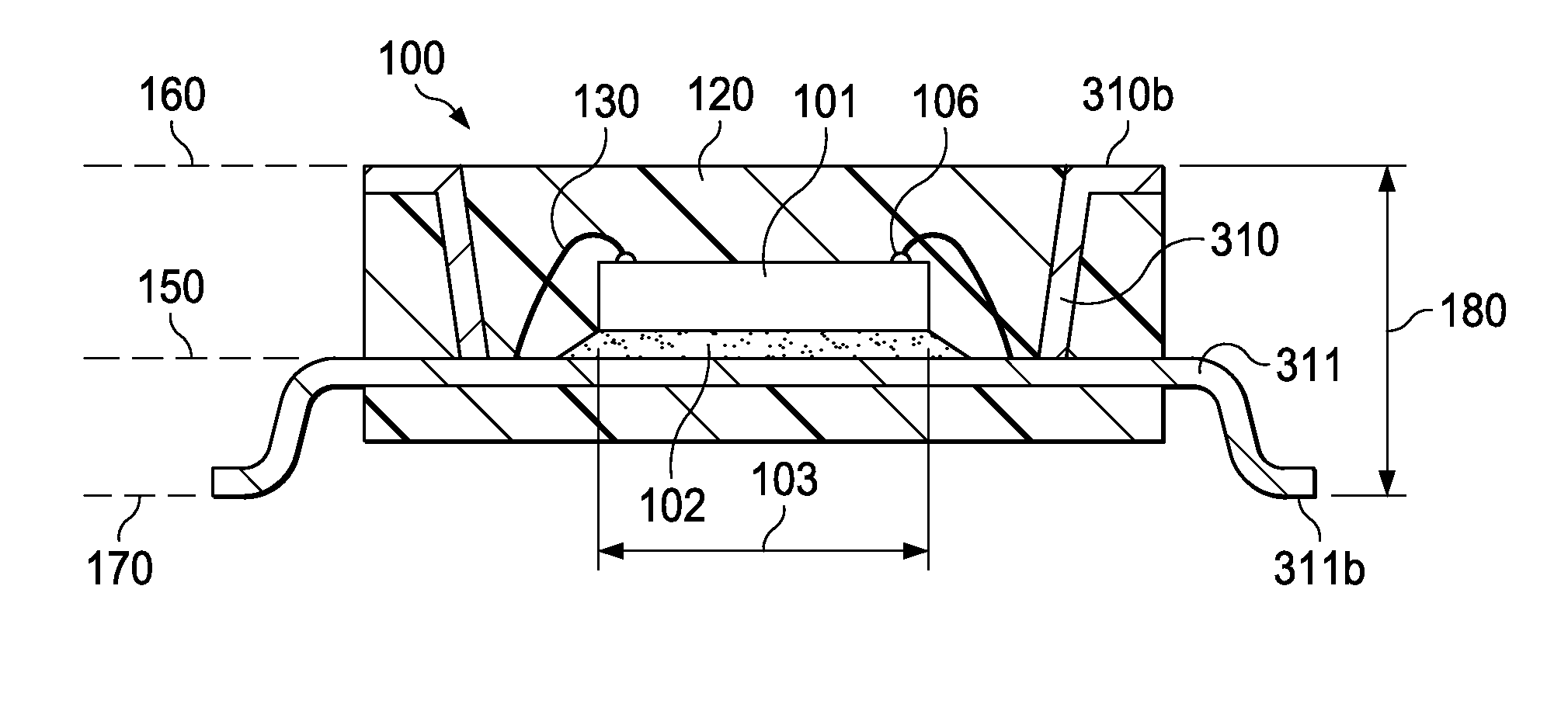
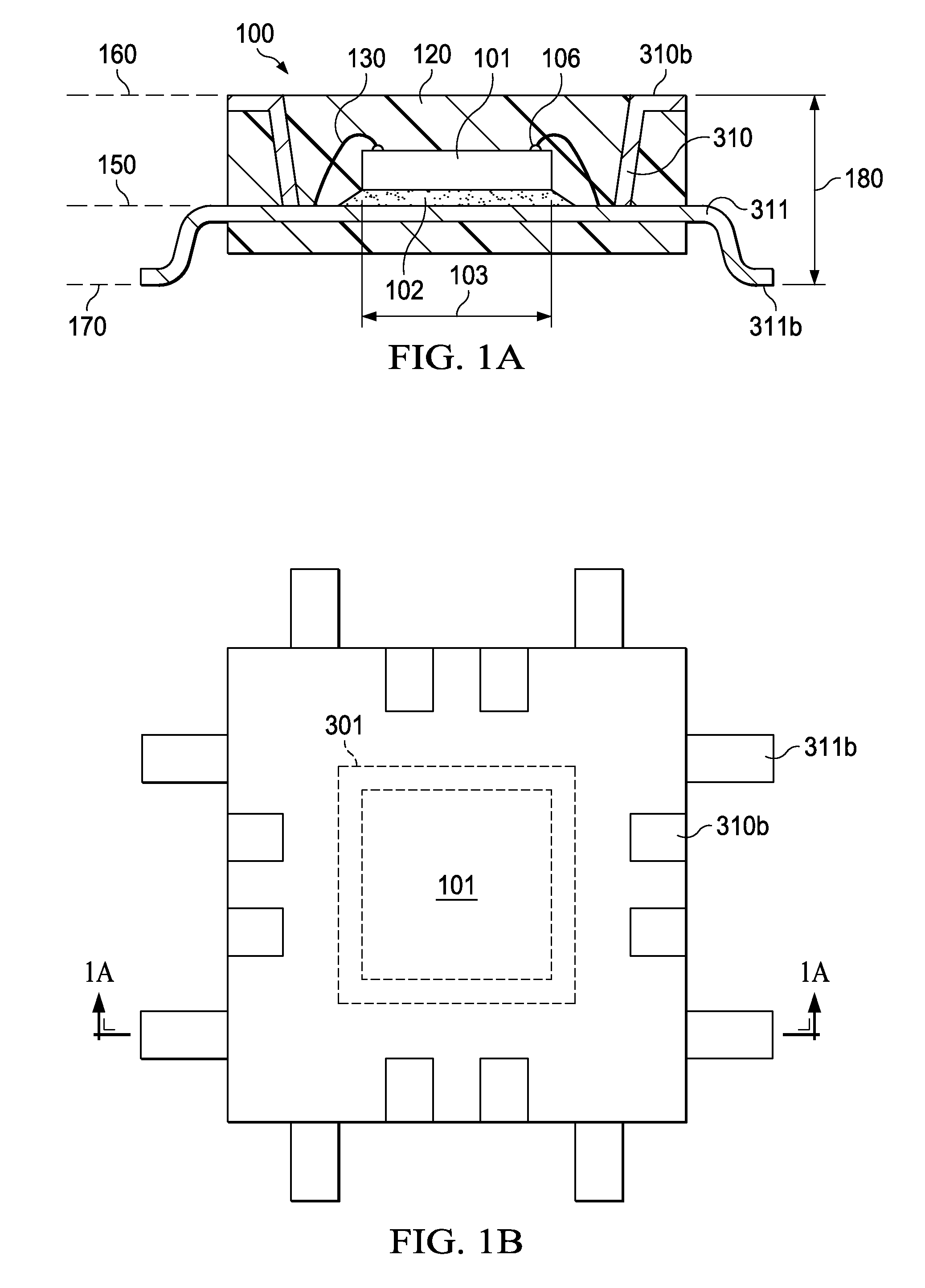
[0043]FIG. 1A illustrates an exemplary embodiment of the invention, a packaged device generally designated 100. The device includes a semiconductor chip 101 with terminals 106; chip 101 is embedded in an insulating package 120. A large variety of chips with a wide range of sizes and shapes may be assembled as shown in FIG. 1; an exemplary chip may be square-shaped with a side length 103 of about 4 mm. Device 100 includes a leadframe with elongated leads from the central region of the device to peripheral regions of the device; consequently, each lead has a central lead end and a peripheral lead end. The central lead ends are in the proximity of chip 101. The terminals 106 of chip 101 may be connected by bonding wires 130 (preferably copper or gold) to the central lead ends; alternatively, terminals 106 may be connected by solder bumps to the central lead ends.

[0044]An example of a starting leadframe suitable for the forming steps of the invention is displayed in FIG. 3A, which shows...


PUM


Abstract

A semiconductor device (100) with a leadframe having first (310) and second (311) leads with central and peripheral ends, the central ends in a first horizontal plane (150). The first leads have peripheral ends (310b) in a second horizontal plane spaced (160) from the first plane and the second leads having peripheral ends in a third horizontal plane (170). A semiconductor chip (101) is connected to the central lead ends. A package (120) encapsulates the chip and the central ends of the first and second leads, leaving the peripheral ends of the first and second leads un-encapsulated, wherein the packaged device has lead ends as terminals on the second and third horizontal plane.

Description

FIELD OF THE INVENTION[0001]The present invention is related in general to the field of semiconductor devices and processes, and more specifically to leadframe-based semiconductor packages with terminals on top and bottom surfaces, and methods to fabricate these packages.DESCRIPTION OF RELATED ART[0002]Semiconductor devices stacked as package-on-package (PoP) products have been introduced in the electronics market more than two decades ago. Stacking packages offers significant advantages by reducing device footprints on circuit boards. Stacking can also be used to improve testability, for instance by permitting separate testing of logic and memory packages before they are assembled as a stacked PoP unit. In other instances, electrical performance may be improved due to shortened interconnections between associated packages. A successful strategy for stacking packages shortens the time-to-market of innovative products by utilizing available devices of various capabilities (such as pr...

Claims


Application Information

Patent Timeline
IPC IPC(8): H01L23/495H01L21/56
CPCH01L21/56H01L23/49575H01L2224/32245H01L2224/48091H01L2224/48247H01L2224/49171H01L2224/73204H01L2224/73265H01L2224/92247H01L23/49541H01L23/49551H01L23/49572H01L21/4842H01L23/3107H01L2924/1461H01L2224/05554H01L2924/181H01L2224/16245H01L2924/00014H01L2924/00H01L2924/00012
Inventor MIYAZAKI, HIROSHI
Owner TEXAS INSTR INC
Why Eureka
Try Eureka