Methods for processing substrates

a technology of substrates and processing methods, applied in the direction of watering devices, other domestic articles, semiconductor/solid-state device details, etc., can solve the problems of inability to apply high-temperature process and damage to wafers

Active Publication Date: 2014-07-31
SAMSUNG ELECTRONICS CO LTD
View PDF10 Cites 20 Cited by
  • Summary
  • Abstract
  • Description
  • Claims
  • Application Information

AI Technical Summary

Benefits of technology

[0006]The present inventive concept provides a method for processing a substrate in which a carrier can be bonded to a wafer with thermal stability.

Problems solved by technology

UV radiation is applied to the glue layer in order to use the UV curable adhesive, but the wafer can be damaged from the UV radiation.
If a thermoplastic adhesive is adopted as the glue layer, a high temperature process cannot be applied due to poor thermal stability.

Method used


Image

  • Methods for processing substrates
  • Methods for processing substrates
  • Methods for processing substrates

Examples


Embodiment Construction

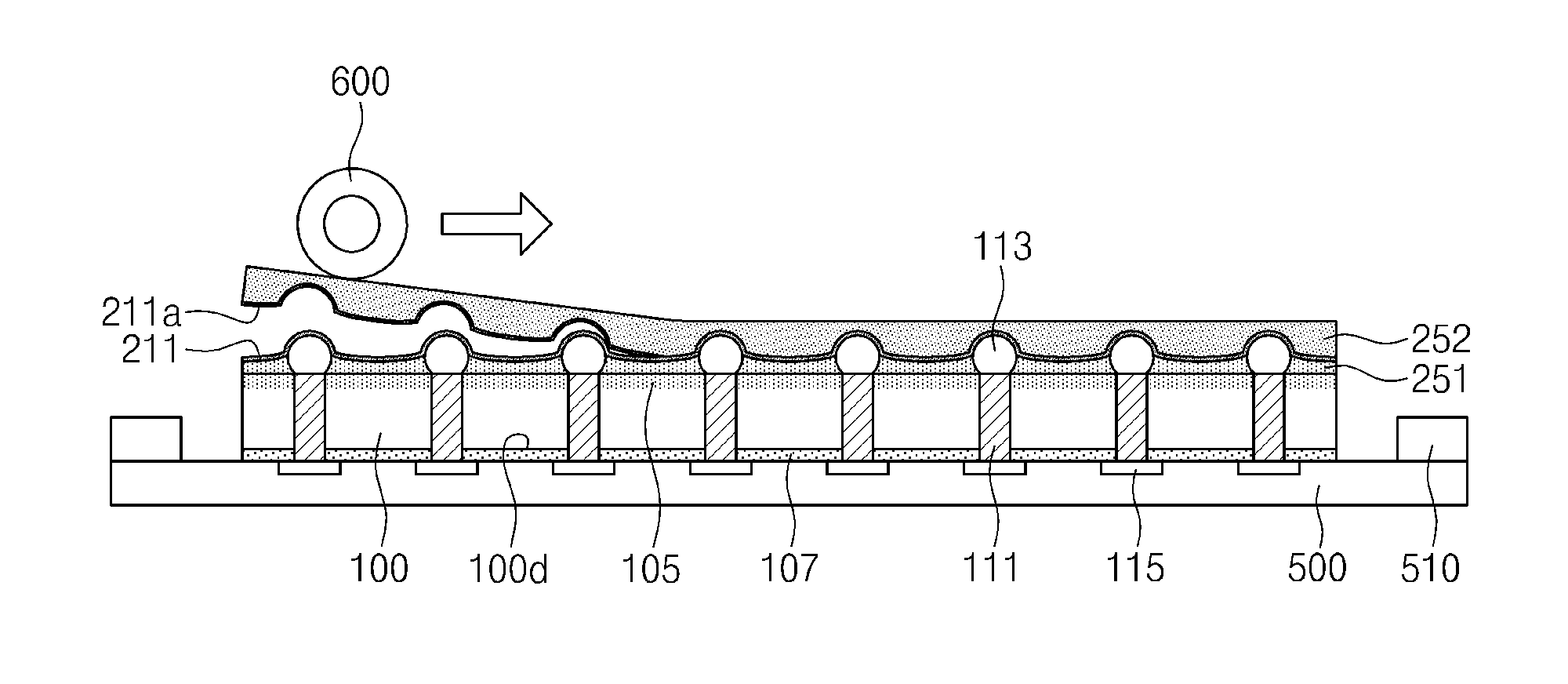
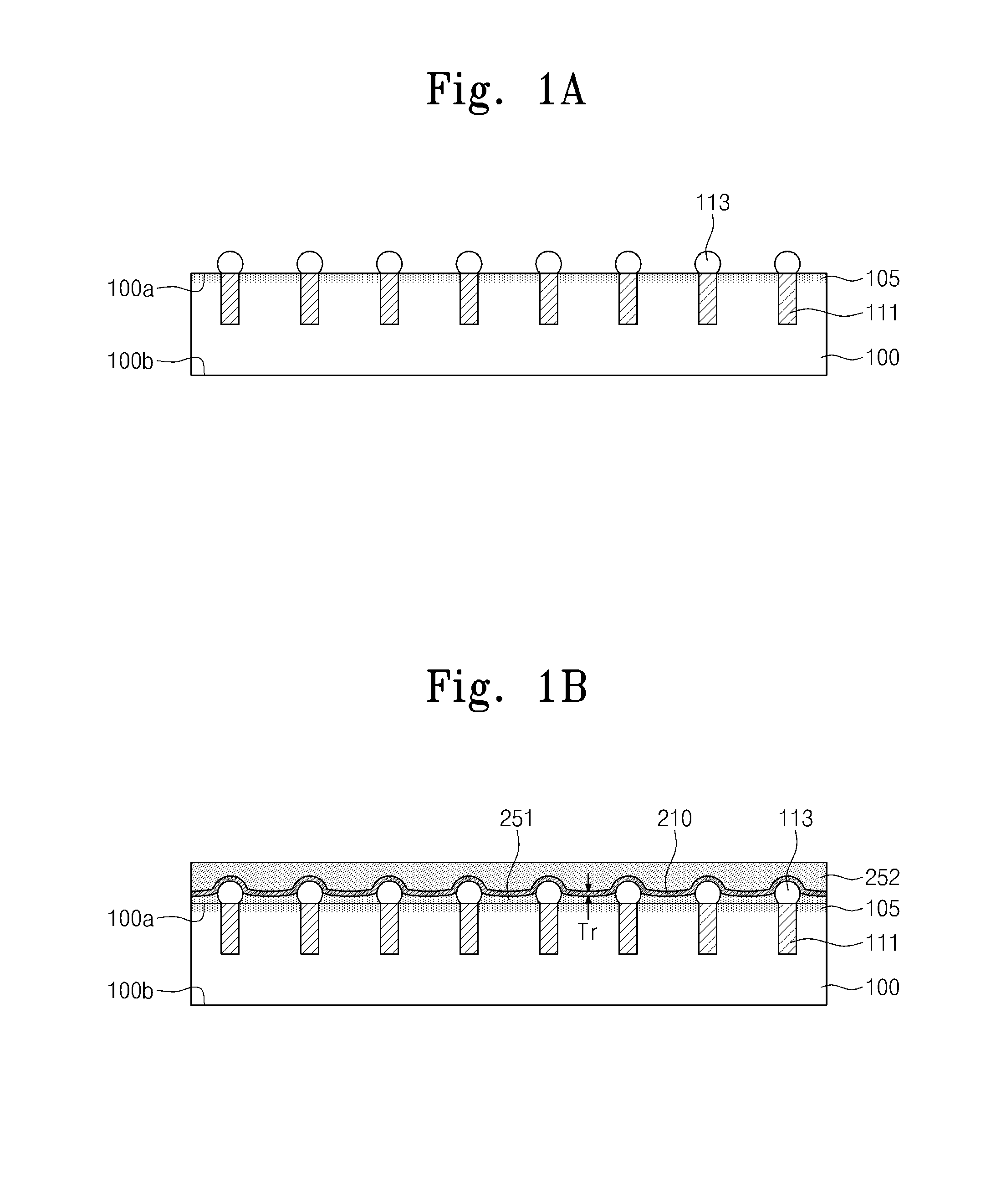
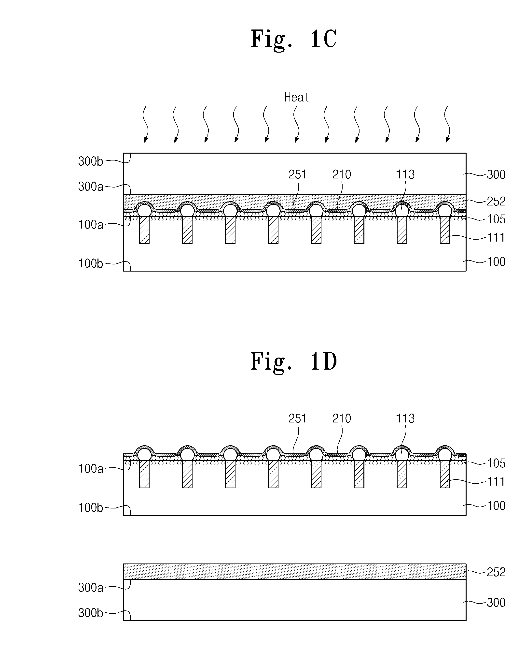
[0044]Reference will now be made in detail to the embodiments of the present general inventive concept, examples of which are illustrated in the accompanying drawings. Example embodiments, may, however, be embodied in many different forms and should not be construed as being limited to the embodiments set forth herein; rather, these example embodiments are provided so that this disclosure will be thorough and complete, and will fully convey the scope of example embodiments of the inventive concept to those of ordinary skill in the art. In the drawings, the thicknesses of layers and regions are exaggerated for clarity. Like reference numerals in the drawings refer to the like elements throughout. The embodiments are described below in order to explain the present general inventive concept while referring to the figures.

[0045]FIGS. 1A to 1K are cross sectional views illustrating an example of a method for processing a substrate, according to an embodiment of the present inventive conc...


PUM


Abstract

A method for processing substrates includes providing a bonding layer between a substrate and a carrier to bond the substrate to the carrier, processing the substrate while the substrate is supported by the carrier, and removing the bonding layer to separate the substrate from the carrier. The bonding layer may include a thermosetting release layer and thermosetting glue layers, wherein at least one of the thermosetting glue layers is provided on each side of the thermosetting release layer.

Description

CROSS-REFERENCE TO RELATED APPLICATIONS[0001]This application claims the benefit of priority under 35 U.S.C. §119 to Korean Patent Application 10-2013-0008692, filed on Jan. 25, 2013, the content of which is incorporated herein in its entirety by reference.BACKGROUND[0002]1. Field[0003]An embodiment of the present inventive concept relates to methods of processing substrates and, more particularly, to methods of thinning wafers.[0004]2. Description of the Related Art[0005]In manufacturing semiconductor process, a wafer is bonded to a carrier with glue and release layers therebetween in order to thin the wafer by a back lap process. An ultraviolet (UV) curable adhesive is generally used as the glue layer. UV radiation is applied to the glue layer in order to use the UV curable adhesive, but the wafer can be damaged from the UV radiation. If a thermoplastic adhesive is adopted as the glue layer, a high temperature process cannot be applied due to poor thermal stability. Therefore, the...

Claims


Application Information

Patent Timeline
Patent Type & Authority Applications(United States)
IPC IPC(8): H01L21/304H01L21/683
CPCH01L21/6836H01L21/304H01L21/6835H01L2221/68318H01L2221/68327H01L2221/6834H01L2221/68381H01L2224/0401H01L2924/12042H01L2924/181Y10S438/977H01L2924/00A01G25/09A01G25/14B05B3/12B05B15/62B32B37/1284B32B37/18B32B37/24B32B37/26B32B38/04B32B38/10B32B38/162B32B2037/268B32B2315/08B32B2457/14H01L21/02057H01L21/02126H01L21/76898H01L24/03H01L24/14H01L2221/68363H01L2221/68372H01L2224/05025H01L2224/13023
Inventor LEE, CHUNGSUNAHN, JUNG-SEOKCHOI, KWANG-CHULKANG, UN-BYOUNGKIM, JUNG-HWANSOHN, JOONSIKLEE, JEON IL
Owner SAMSUNG ELECTRONICS CO LTD
Why Eureka
Try Eureka