Method of manufacturing electronic device, electronic device, electronic apparatus, and moving object

a manufacturing method and technology for electronic devices, applied in the direction of casings/cabinets/drawers, instruments, casings/cabinets/drawers, etc., can solve the problems of increasing the number of man-hours required for sealing, not easy to control the dimensions of unwelded portions and the like stably, and achieve excellent reliability

Active Publication Date: 2014-07-31
SEIKO EPSON CORP
View PDF3 Cites 9 Cited by
  • Summary
  • Abstract
  • Description
  • Claims
  • Application Information

AI Technical Summary

Benefits of technology

[0035]According to the moving object, a movin...

Problems solved by technology

However, in the bonding methods disclosed in JP-A-2000-223604 and JP-A-2002-359311, since the lid and the peripheral edge of the opening portion are welded while some parts are left, and after the deaeration, the unwelded portions are welded, it is not easy to control the dimensions of the unwelded portions and the like stably.
Also, since the deaeration from a small gap between the unwelded portions is perfo...

Method used


Image

  • Method of manufacturing electronic device, electronic device, electronic apparatus, and moving object
  • Method of manufacturing electronic device, electronic device, electronic apparatus, and moving object
  • Method of manufacturing electronic device, electronic device, electronic apparatus, and moving object

Examples


first embodiment

of Electronic Device

[0053]First, an embodiment of a vibrator as a first embodiment of an electronic device manufactured by applying a method of manufacturing an electronic device according to the invention will be described.

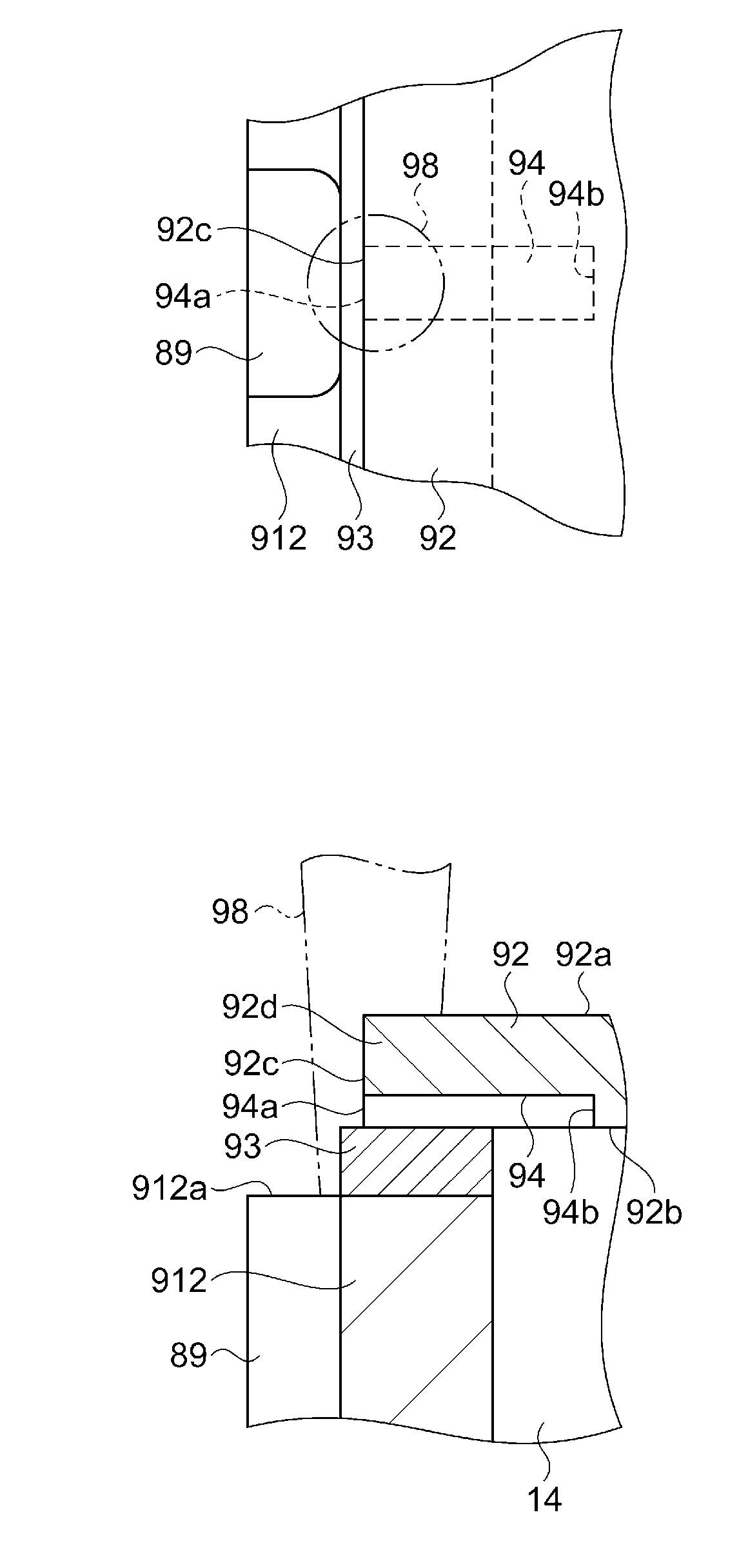
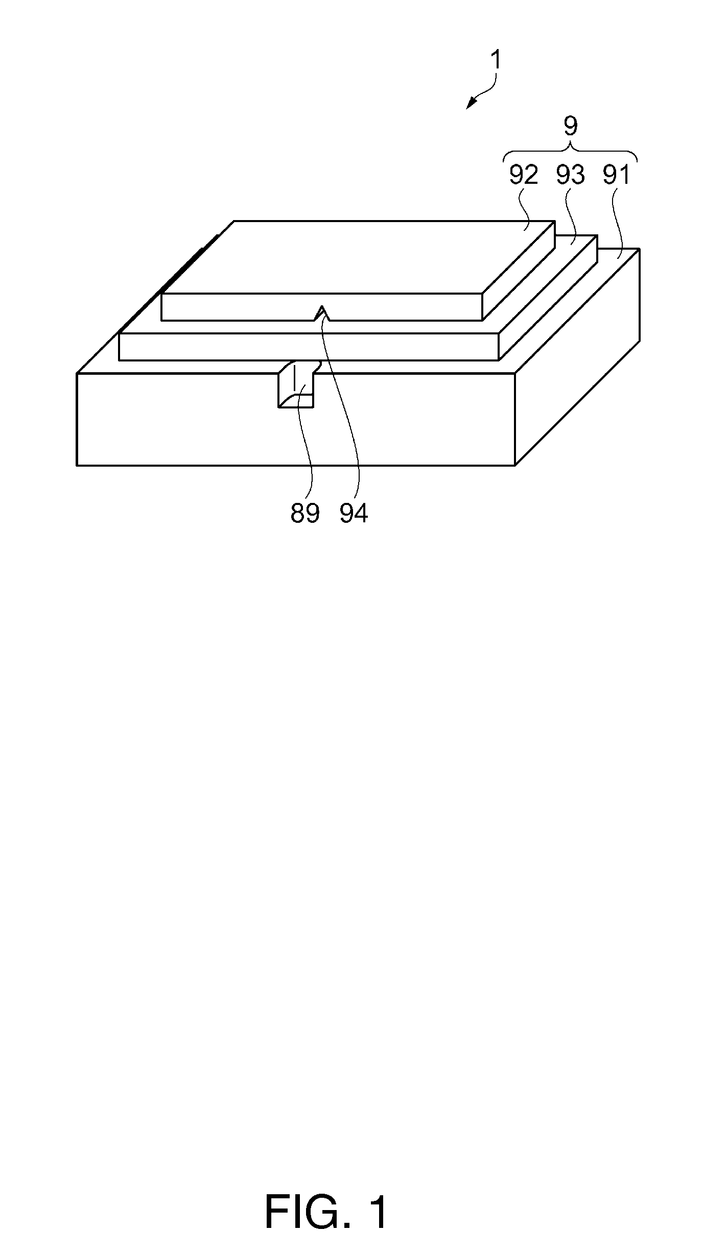
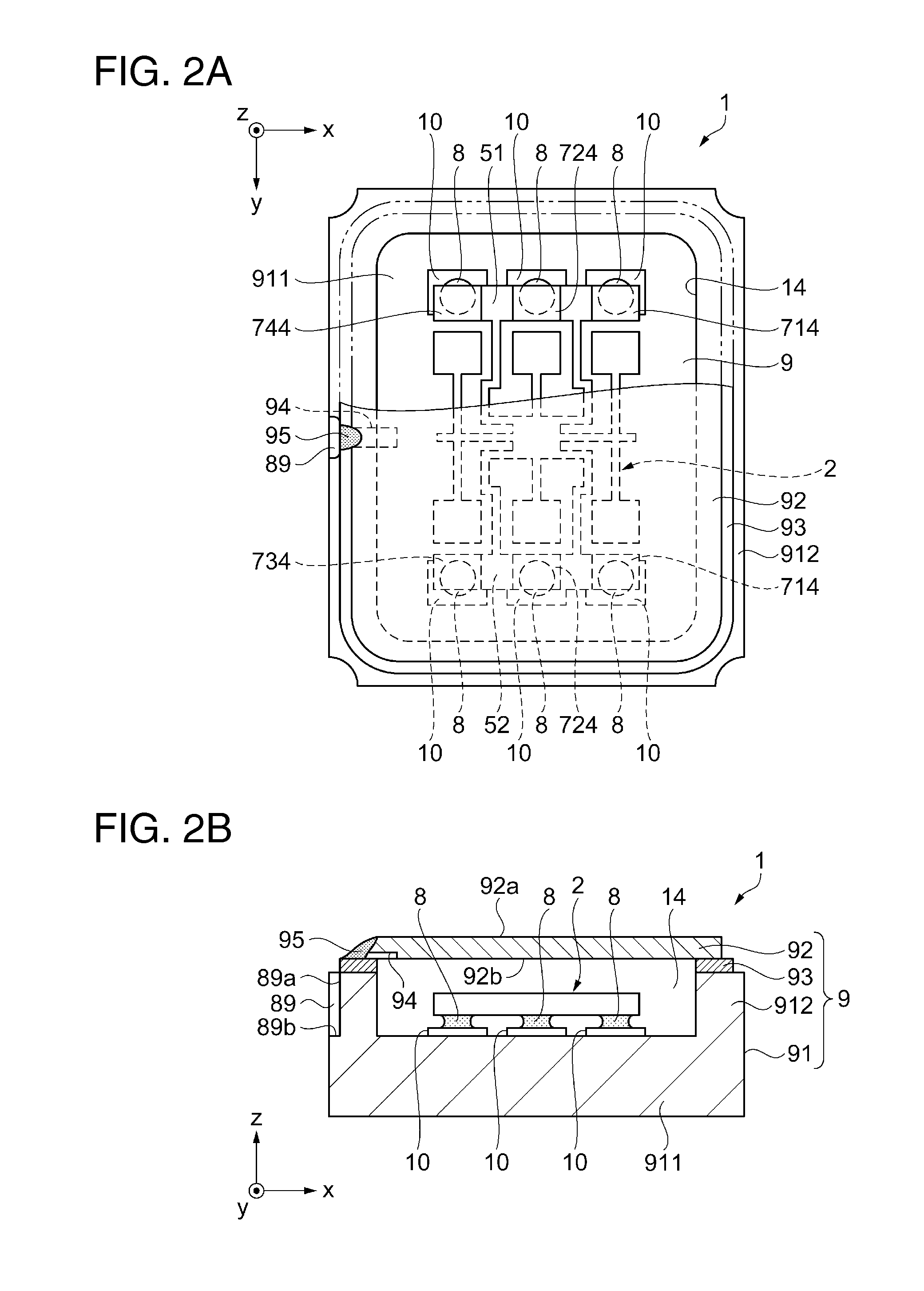
[0054]FIG. 1 is a schematic perspective view showing the vibrator as the first embodiment of the electronic device according to the invention. FIGS. 2A and 2B are schematic views showing the vibrator as the first embodiment of the electronic device according to the invention, and FIG. 2A is a plan view and FIG. 2B is a front cross-sectional view. FIG. 3 is a plan view showing a gyro element as an electronic component including the vibrator shown in FIGS. 2A and 2B. As shown in FIGS. 2A and 2B, an x axis, a y axis, and a z axis are shown below as three axes perpendicular to one another, and the z axis coincides with a thickness direction of the vibrator. In addition, a direction parallel to the x axis is referred to as an “x-axis direction (second direction)”, a d...

modification examples

of Bonding Process and Bonding Structure

[0099]In the above-described first embodiment, the bonding method in which seam welding is performed by the roller electrodes 97 of the seam welding machine using the seam ring 93 that is a ring-shaped metal frame as the bonding material for bonding the base 91 and the lid 92 has been described. However, another bonding method can be used. That is, as another bonding method, a bonding method (so-called direct seam method) in which a brazing material such as a silver brazing material as a bonding material is arranged on the upper surface of the frame-shaped side wall 912 of the base 91 or the surface of the lid 92, and the brazing material is melted by the roller electrodes 97 of the seam welding machine to bond the lid 92 and the base 91 using the molten metal brazing material can be applied. In this case, the metal brazing material may be melted by an energy beam such as a laser or an electron beam. As still another bonding method, a bonding ...

second embodiment

of Electronic Device

[0119]Next, as a second embodiment of the electronic device, an embodiment of a gyro sensor will be described with reference to FIG. 11. FIG. 11 is a front cross-sectional view schematically showing the gyro sensor. In the embodiment, the same reference numerals are attached to the same configurations as in the first embodiment and the descriptions thereof will be omitted in some cases.

[0120]A gyro sensor 200 includes the gyro element 2 as the electronic component, an IC 112 as a circuit element, a package (base) 111 as a housing container, and the lid 92 as the lid body. The package 111 formed of ceramic or the like has a third substrate 125c, a second substrate 125b, and a first substrate 125a, which are laminated, a frame-shaped side wall 115 which is provided in a surface peripheral edge portion of the first substrate 125a, and a frame-shaped side wall 120 which is provided in a surface peripheral edge portion of the third substrate 125c.

[0121]On the upper s...


PUM


Abstract

A method of manufacturing an electronic device in which an inner space for housing a gyro element is formed between a base and a lid and the base and the lid are bonded includes bonding the base and the lid in which a groove is provided on a surface to be bonded with the base so that the inner space communicates with the outside by not bonding the inner surface of the groove to the base and to position the groove around a concave portion provided on a side surface of the base, and closing a communication portion by irradiating a laser beam to the lid in the communication portion.

Description

BACKGROUND[0001]1. Technical Field[0002]The present invention relates to a method of manufacturing an electronic device, an electronic device, an electronic apparatus, and a moving object.[0003]2. Related Art[0004]In recent years, portable type electronic apparatuses have been popularized and along with the popularization, there has been an increasing demand for a reduction in size, weight and cost of the electronic apparatuses. Therefore, there has been an increasing demand for a reduction in size and cost of electronic components used in the electronic apparatuses while high accuracy is maintained. Particularly, since vibration characteristics are maintained in vibration devices in which a vibration element is housed in a package by airtightly maintaining a space for housing the vibration element, various sealing techniques have been proposed.[0005]For example, in bonding methods disclosed in JP-A-2000-223604 and JP-A-2002-359311, a lid that covers an opening portion of a space fo...

Claims


Application Information

Patent Timeline
IPC IPC(8): B23K26/26B23K11/06B23K1/005H05K5/03
CPCB23K26/26H05K5/03B23K11/061B23K1/0056G01C19/5783H01L2224/16225H01L2924/16195H05K5/066
Inventor AOKI, SHINYAMATSUZAWA, JUICHIROKAWAUCHI, OSAMUMIKAMI, MASARU
Owner SEIKO EPSON CORP
Why Eureka
Try Eureka