Trench metal oxide semiconductor field effect transistor with embedded schottky rectifier using reduced masks process

a technology of metal oxide semiconductor and field effect transistor, which is applied in the field of metal oxide semiconductor field effect transistor with embedded schottky rectifier using reduced masks process, to achieve the effects of improving avalanche capability, reducing masking, and increasing junction depth

Inactive Publication Date: 2014-07-31
FORCE MOS TECH CO LTD
View PDF7 Cites 9 Cited by
  • Summary
  • Abstract
  • Description
  • Claims
  • Application Information

AI Technical Summary

Benefits of technology

The present invention is about a new type of transistor called a trench MOSFET with embedded Schottky rectifier. This transistor has several technical features. First, it uses a special process to form the source regions, which results in higher doping concentration and greater junction depth near the sidewalls of the source-body contacts. This makes it more difficult for the transistor to turn on and improves its avalanche capability. Second, the transistor has at least one anti-punch through implant region to enhance its ability to resist electrical current and improve its performance. Third, the transistor has a doped island of the second conductivity type to reduce electric field near the embedded Schottky rectifier and further improve its performance. Fourth, the transistor has at least one trenched gate contact that has a shallower depth than the source-body contacts to avoid short-circuiting between the gate and drain. Overall, this new transistor design has improved performance and reliability.

Problems solved by technology

Moreover, the lower doping concentration near the channel region added the difficulties for the parasitic bipolar transistor to be turned on, avoiding the UIS failure issue and improving the avalanche capability.

Method used


Image

  • Trench metal oxide semiconductor field effect transistor with embedded schottky rectifier using reduced masks process
  • Trench metal oxide semiconductor field effect transistor with embedded schottky rectifier using reduced masks process
  • Trench metal oxide semiconductor field effect transistor with embedded schottky rectifier using reduced masks process

Examples


Embodiment Construction

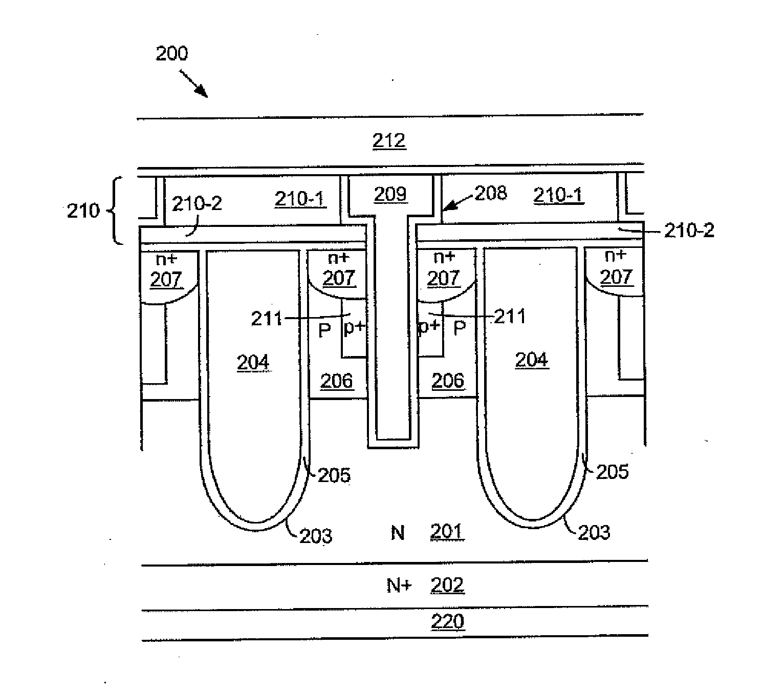
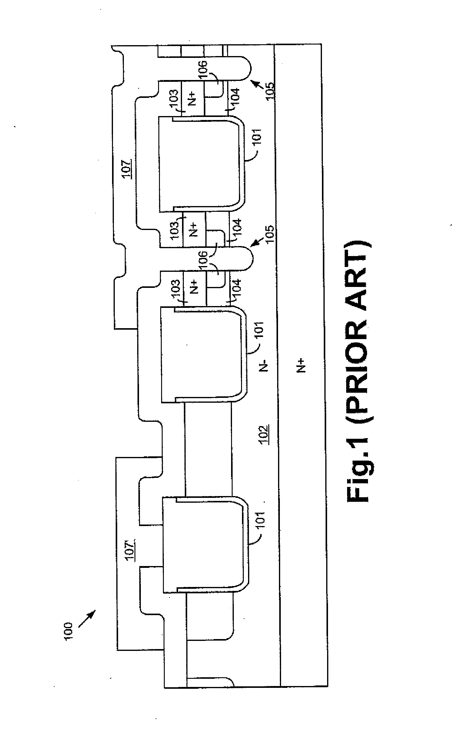
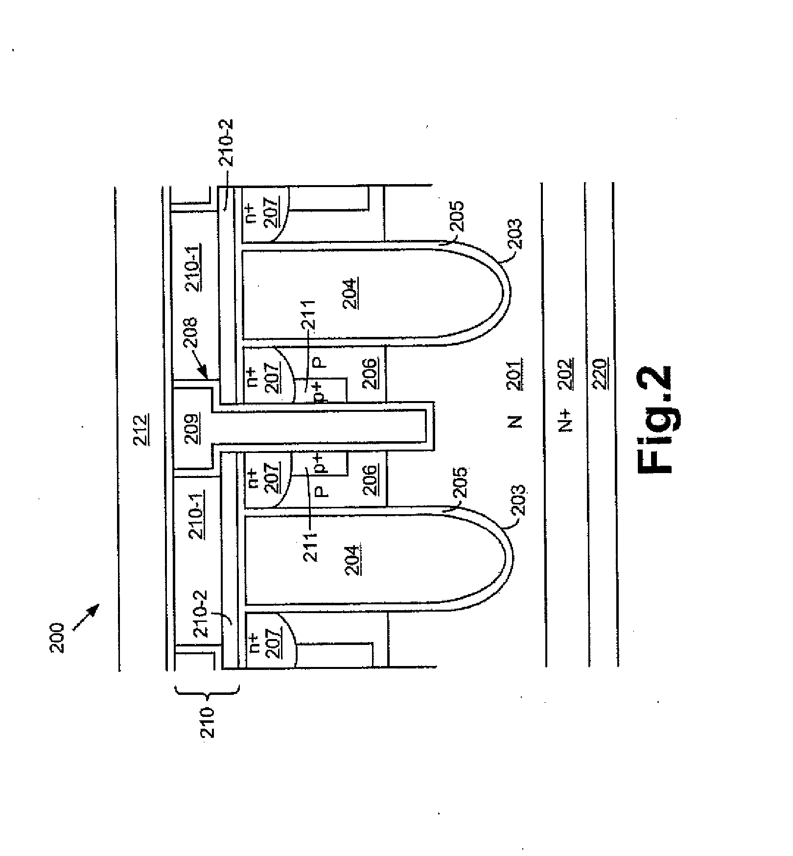
[0028]In the following Detailed Description, reference is made to the accompanying drawings, .which forms a part thereof, and in which is shown by way of illustration specific embodiments in which the invention may be practiced. In this regard, directional terminology, such as “top”, “bottom”, “front”, “back”, etc., is used with reference to the orientation of the Figure(s) being described. Because components of embodiments can be positioned in a number of different orientations, the directional terminology is used for purpose of illustration and is in no way limiting. It is to be understood that other embodiments may be utilized and structural or logical changes may be make without departing from the scope of the present invention. The following detailed description, therefore, is not to be taken in a limiting sense, and the scope of the present invention is defined by the appended claims. It is to be understood that the features of the various exemplary embodiments described herei...


PUM

PropertyMeasurementUnit
doping concentrationaaaaaaaaaa
inductanceaaaaaaaaaa
leakage currentaaaaaaaaaa

Abstract

A trench MOSFET with embedded schottky rectifier having at least one anti-punch through implant region using reduced masks process is disclosed for avalanche capability enhancement and cost reduction. The source regions have a higher doping concentration and a greater junction depth along sidewalls of the trenched source-body contacts than along adjacent channel regions near the gate trenches.

Description

FIELD OF THE INVENTION[0001]This invention relates generally to the cell structure, device configuration and fabrication process of power semiconductor devices. More particularly, this invention relates to a novel and improved cell structure, device configuration and improved fabrication process of a trench metal oxide semiconductor field effect transistor (MOSFET, the same hereinafter) with embedded schottky rectifier using reduced masks process.BACKGROUND OF THE INVENTION[0002]Conventional technologies for manufacturing trench semiconductor power devices are continuously challenged to further reduce the manufacturing cost by reducing the number of masks applied in the manufacturing process. For example, for a trench MOSFET with embedded schottky rectifier, simplifying the manufacturing process and cutting down the manufacturing cost without degrading performance is mainly required by device designing and manufacturing.[0003]Prior art U.S. Pat. No. 7,285,822 disclosed an N-channel ...

Claims


Application Information

Patent Timeline
Patent Type & Authority Applications(United States)
IPC IPC(8): H01L29/66
CPCH01L21/26586H01L29/404H01L2924/0002H01L29/407H01L29/41766H01L29/4236H01L29/42368H01L29/456H01L29/7813H01L29/47H01L29/66734H01L29/7806H01L29/7811H01L29/0623H01L29/0869H01L29/0878H01L29/1095H01L29/66666H01L29/872H01L2924/00
Inventor HSIEH, FU-YUAN
Owner FORCE MOS TECH CO LTD
Why Eureka
Try Eureka