Low impedance interface circuit to maximize bandwidth and provide bias control

a low impedance, bias control technology, applied in the field of processing analog signals, can solve the problems of increasing manufacturing complexity and cost, and increasing the complexity of readout electronics, so as to achieve the effect of maximizing bandwidth and providing bias control

Active Publication Date: 2014-08-14
GENERAL ELECTRIC CO
View PDF1 Cites 24 Cited by
  • Summary
  • Abstract
  • Description
  • Claims
  • Application Information

AI Technical Summary

Problems solved by technology

However, the transmission of analog signals from the SiPM for processing can present problems.
Therefore, many individual signal lines may be required to carry the signals, which increases complexity in readout electronics, manufacturing complexity and cost.
Furthermore, the quality of the signal is more likely to deteriorate as the size and complexity of the SiPM increases.

Method used


Image

  • Low impedance interface circuit to maximize bandwidth and provide bias control
  • Low impedance interface circuit to maximize bandwidth and provide bias control
  • Low impedance interface circuit to maximize bandwidth and provide bias control

Examples


Embodiment Construction

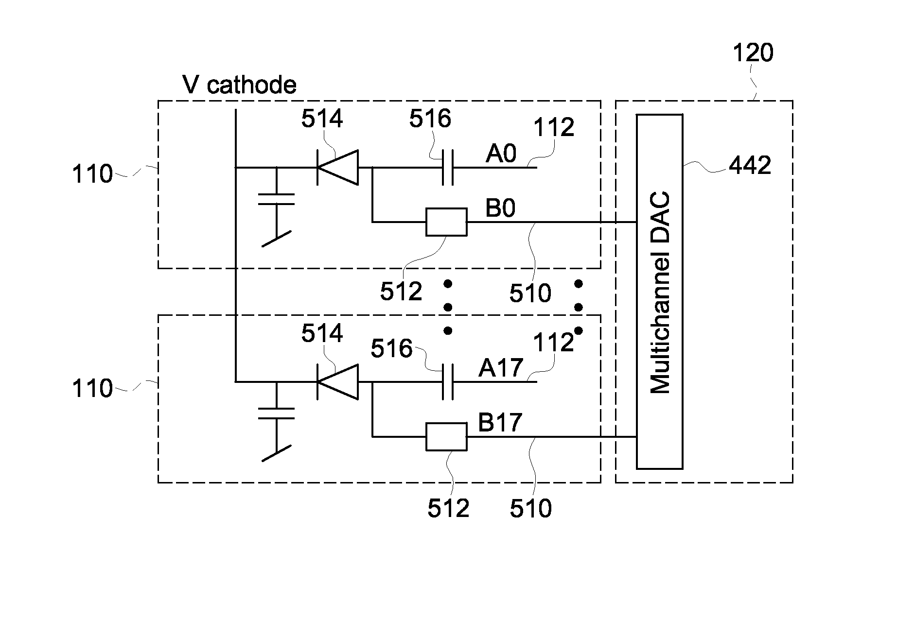
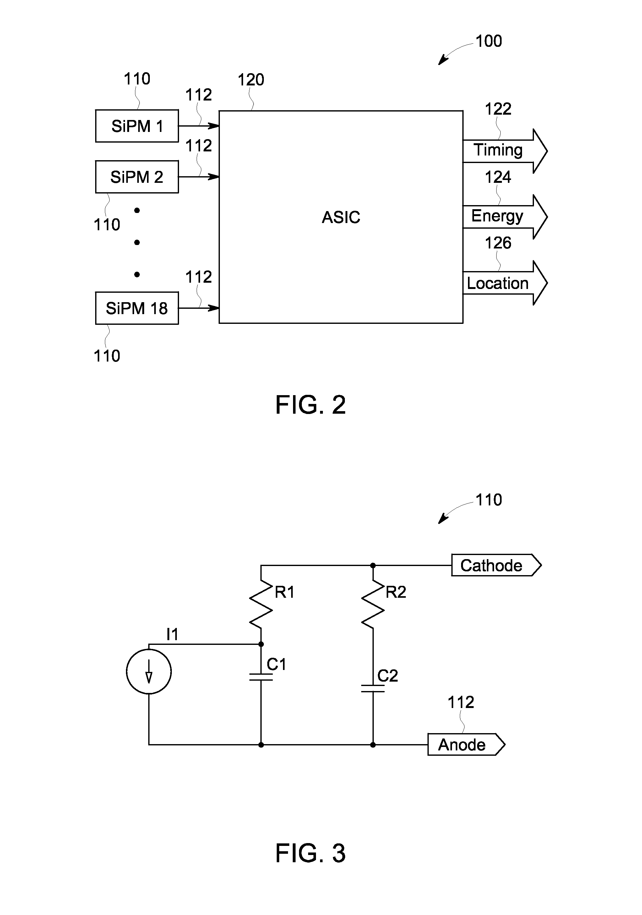
[0022]Exemplary embodiments are directed to apparatus and methods of processing analog signals generated by one or more SiPMs. In one embodiment, a multichannel readout front-end application-specific integrated circuit (ASIC) interfaces with an array of SiPMs in a Positron Emission Tomography (PET) system. The ASIC is configured to provide information on the timing, energy, and location of events in each SiPM to a processing system, as well as the ability to bias each SiPM.

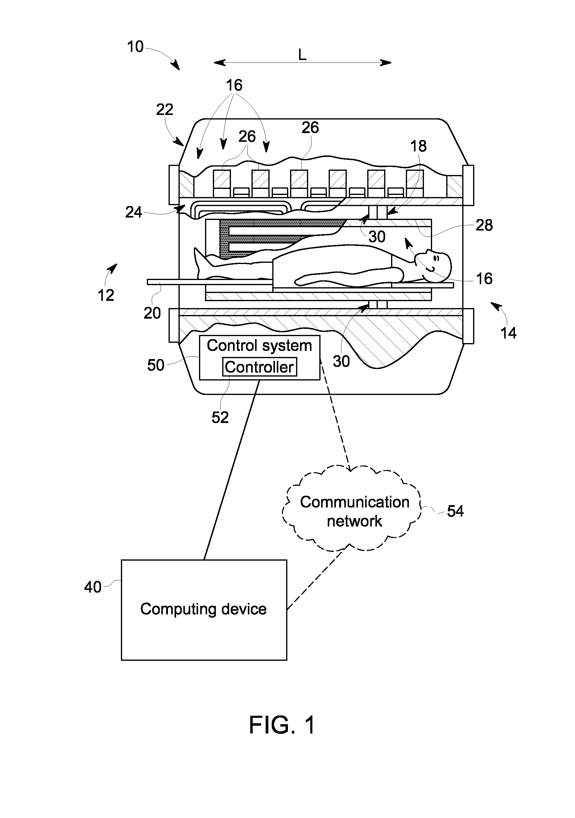
[0023]FIG. 1 depicts one example of a hybrid or combined Positron Emission Tomography (PET)—Magnetic Resonance Imaging (MRI) scanner 10 that can be used in conjunction with various embodiments. The scanner 10 can generally extend longitudinally along a longitudinal axis L from a proximal end 12 to the distal end 14. The scanner 10 can include MRI components 16 forming an MRI scanner portion configured to acquire MR data and / or PET imaging components 18 forming a PET image scanner portion configured to acquire PET ...


PUM


Abstract

A multichannel application specific integrated circuit (ASIC) for interfacing with an array of photodetectors in a positron emission tomography (PET) imaging system includes a front end circuit configured to be coupled to the photodetectors and to receive discrete analog signals therefrom. The ASIC further includes a time discriminating circuit operably coupled to the front end circuit and configured to generate a hit signal based on a combination of the discrete analog signals, and an energy discriminating circuit operably coupled to the front end circuit and configured to generate a summed energy output signal based on each of the discrete analog signals and summed row and column output signals based on each of the discrete analog signals. The summed energy output signal represents an energy level of the detected radiation in the array of photodetectors, and the summed row and column output signals represent a location of the detected radiation.

Description

FIELD[0001]This disclosure relates generally to imaging, and more particularly, to apparatus and methods of processing analog signals generated by solid state photomultiplier devices.BACKGROUND[0002]A silicon photomultiplier (SiPM) is an array of passively quenched Geiger-mode avalanche photodiodes (APD) for detecting impinging photons. SiPM can provide information about certain parameters, such as the time of the impingement event, the energy associated with the event, and the position of the event within the detector. These parameters can be determined through processing algorithms applied to the analog signals generated by the SiPM. Some conventional SiPMs can produce very fast signals, which provides a high degree of timing accuracy.[0003]SiPMs provide certain advantages over conventional photomultiplier tubes (PMTs), and are therefore being used in many applications, including Positron Emission Tomography (PET) for medical imaging. These advantages include better photon detecti...

Claims


Application Information

Patent Timeline
Patent Type & Authority Applications(United States)
IPC IPC(8): G01T1/29
CPCG01T1/2985A61B6/037G01R33/481G01T1/1603G01T1/1647
Inventor GUO, JIANJUNDOLINSKY, SERGEI IVANOVICHKIM, CHANGLYONGMALANEY, JAMES LINDGRENMCDANIEL, DAVID LEOPETERSON, WILLIAM
Owner GENERAL ELECTRIC CO
Why Eureka
Try Eureka