Film forming method, vacuum processing apparatus, semiconductor light emitting element manufacturing method, semiconductor light emitting element, and illuminating device

a technology manufacturing methods, applied in the direction of polycrystalline material growth, chemically reactive gas growth, crystal growth process, etc., can solve the problems of high production cost, difficult to achieve high yield, and single crystal substrates made of a group iii nitride semiconductors are extremely expensive and have not therefore been utilized, so as to improve the light emission characteristics of light emitting elements such as leds and lds. , the effect of small til

Active Publication Date: 2014-08-14
CANON ANELVA CORP
View PDF1 Cites 13 Cited by
  • Summary
  • Abstract
  • Description
  • Claims
  • Application Information

AI Technical Summary

Benefits of technology

[0034]According to the present invention, a Group III nitride semiconductor epitaxial film having small tilt and twist mosaic spreads and also +c polarity can be fabricated on an α-Al2O3 substrate by using

Problems solved by technology

However, a single-crystal substrate made of a Group III nitride semiconductor is extremely expensive and has not therefore been utilized, except in some applications.
However, MOCVD has problems such as requiring a high production cost and having a tendency to develop particles, making it difficult to achieve a high yield.
However, Group III nitride semiconductor thin f

Method used


Image

  • Film forming method, vacuum processing apparatus, semiconductor light emitting element manufacturing method, semiconductor light emitting element, and illuminating device
  • Film forming method, vacuum processing apparatus, semiconductor light emitting element manufacturing method, semiconductor light emitting element, and illuminating device
  • Film forming method, vacuum processing apparatus, semiconductor light emitting element manufacturing method, semiconductor light emitting element, and illuminating device

Examples


embodiment

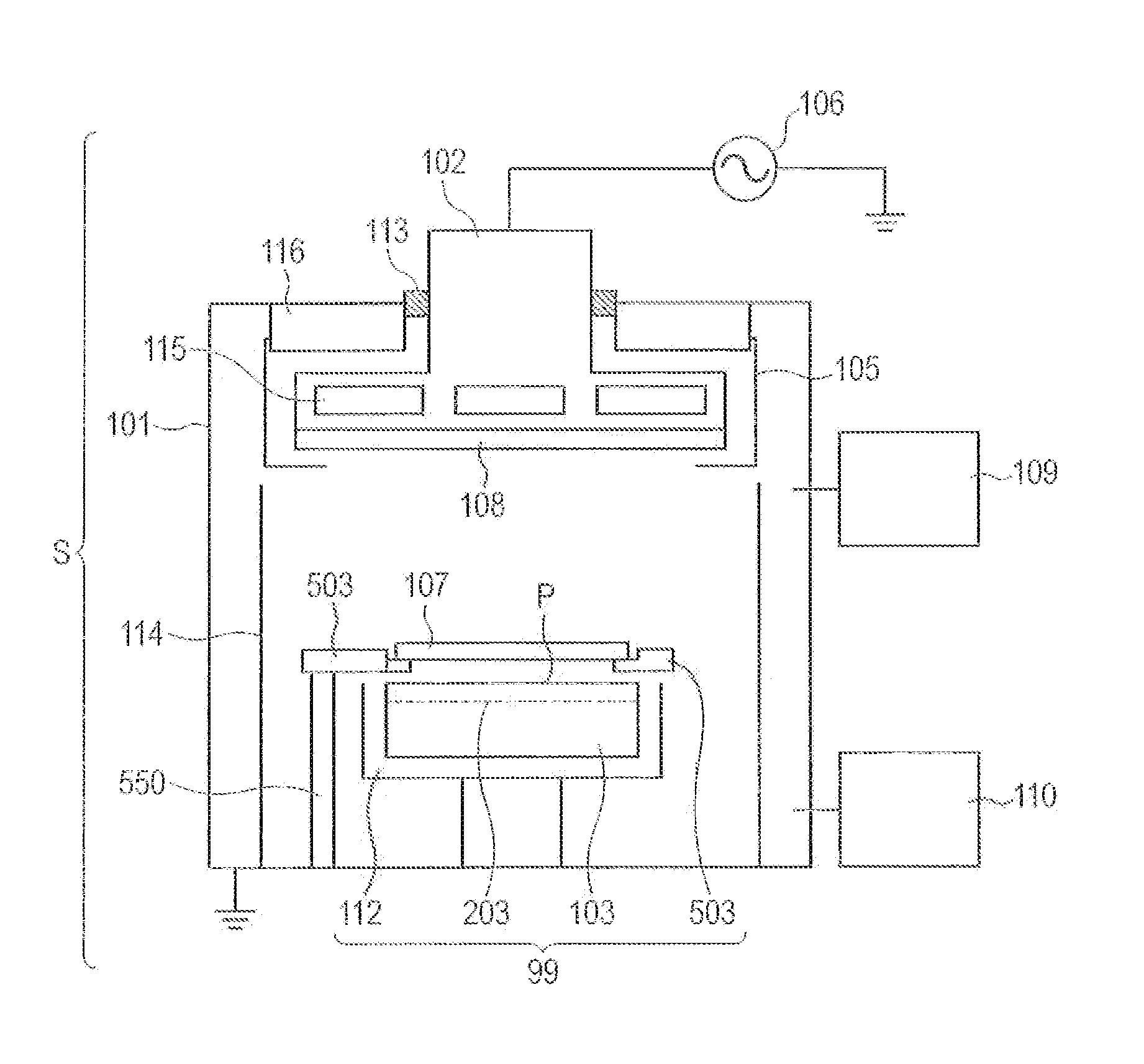
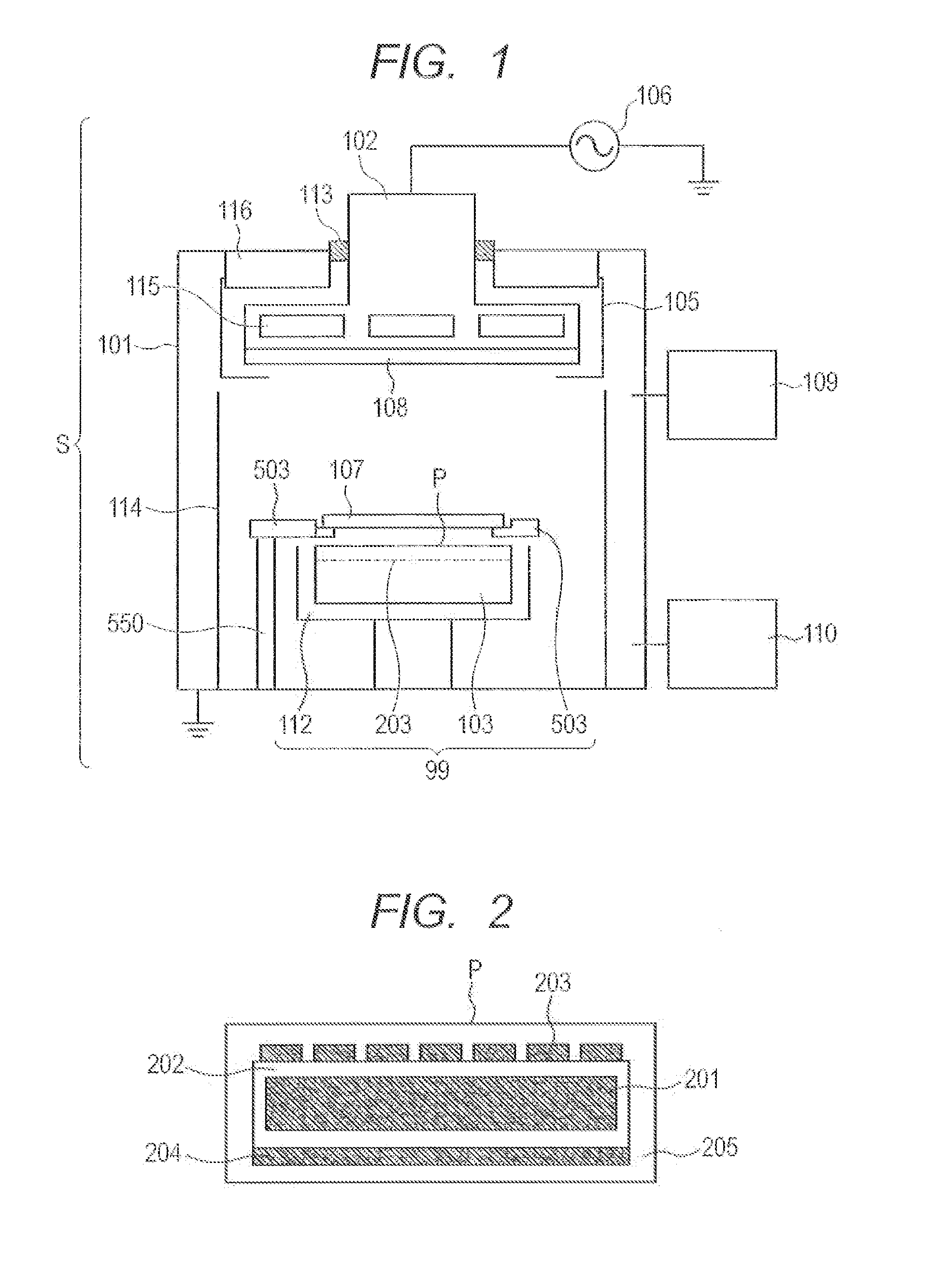
[0052]A main feature according to the present invention is that when a semiconductor thin film having a wurtzite structure (e.g. a Group III nitride semiconductor thin film or ZnO-based semiconductor thin film having a wurtzite structure) is to be epitaxially growth (e.g. a substrate having a non polar surface (described later) such as an α-Al2O3 substrate, a Si substrate or a Ge substrate, and a substrate having a polar surface (described later) such as a 4H—SiC substrate) by such sputtering as radio frequency sputtering, the semiconductor film having the wurtzite structure is formed in a state where the substrate heated by a heater is held away by a predetermined distance from the substrate facing surface of the heater. Hereinbelow, the present invention will be described with reference to the drawings. Note that members and arrangements described below are mere examples embodying the invention and do not limit the present invention. They can be modified in various ways on the bas...

first example

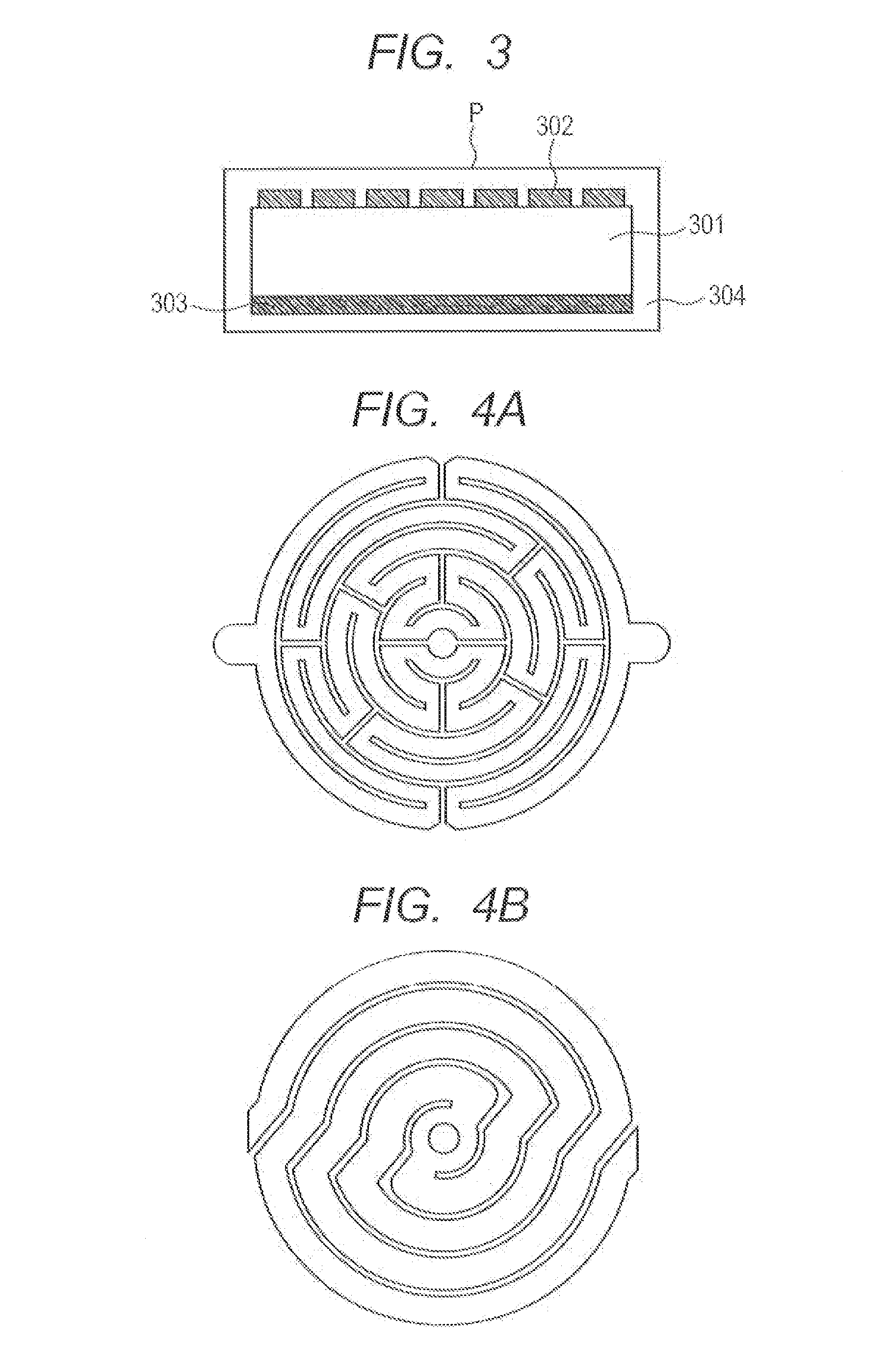
[0106]As a first example of the present invention, description will be given of an example where an AlN film is formed on an α-Al2O3 (0001) substrate by using the method of forming a Group III nitride semiconductor thin film having a wurtzite structure according to one embodiment of the present invention. More specifically, description will be given of an example where an AlN film having a wurtzite structure is formed by using sputtering on an α-Al2O3 (0001) substrate mounted with a gap between the substrate and the substrate facing surface of a heater with the help of a substrate holding device. Note that in this example, the AlN film was formed by using a similar sputtering apparatus to that in FIG. 1. A similar heater structure to that in FIG. 2, a similar heater electrode pattern to that in FIG. 4A, and a similar substrate holding device to that in FIG. 5 were used. Moreover, the gap d1 between the substrate supporting portion 503a and the substrate facing surface P of the heate...

second example

[0116]Next, as a second example of the present invention, description will be given of an example where an AlN film having a wurtzite structure is fabricated as a buffer layer by using the method of forming a Group III nitride semiconductor thin film having a wurtzite structure according to one embodiment of the present invention, and then an undoped GaN film is formed on the buffer layer by using MOCVD.

[0117]An AlN film was formed by using sputtering on an α-Al2O3 (0001) substrate under the same conditions as the first example. Then, the wafer was introduced into a MOCVD apparatus to form an undoped GaN film of a film thickness of 5 μm.

[0118]The surface of the undoped GaN film thus obtained is a mirror surface. XRD measurement in a 2θ / ω scan mode at symmetrical reflection positions showed that the undoped GaN film was orientated in the c-axis direction. Next, XRC measurement in an ω scan mode using GaN (0002) plane as a symmetrical plane, and XRC measurement in a φ scan mode with r...


PUM

PropertyMeasurementUnit
Temperatureaaaaaaaaaa
Structureaaaaaaaaaa
Gravityaaaaaaaaaa

Abstract

In one embodiment of the present invention, a film forming method of epitaxially growing a semiconductor film having a wurtzite structure by sputtering on a substrate for epitaxial growth heated to a desired temperature by using a heater, comprises the following steps. First, the substrate is disposed on a substrate holder including the heater in such a way that the substrate is disposed away from the heater by a predetermined distance. Then, the epitaxial film of the semiconductor film having the wurtzite structure is formed on the substrate in the state where the substrate is disposed away from the heater by the predetermined distance.

Description

CROSS-REFERENCES TO RELATED APPLICATIONS[0001]This application is a continuation application of International Application No. PCT / JP2012 / 006769, filed Oct. 23, 2012, which claims the benefit of Japanese Patent Application No. 2011-236689, filed Oct. 28, 2011. The contents of the aforementioned applications are incorporated herein by reference in their entireties.TECHNICAL FIELD[0002]The present invention relates to a film forming method, a vacuum processing apparatus, a semiconductor light emitting element manufacturing method, a semiconductor light emitting element, and an illuminating device, and particularly relates to a film forming method and a vacuum processing apparatus capable of forming a high-quality epitaxial film, as well as a semiconductor light emitting element manufacturing method, a semiconductor light emitting element, and an illuminating device using such an epitaxial film.BACKGROUND ART[0003]Group III nitride semiconductors are compound semiconductor materials obt...

Claims


Application Information

Patent Timeline
IPC IPC(8): C30B25/10H01L33/18
CPCH01L33/18C30B25/10C30B23/02C30B29/403H01L21/02378H01L21/02381H01L21/0242H01L21/02433H01L21/02458H01L21/0254H01L21/02554H01L33/007
Inventor DAIGO, YOSHIAKI
Owner CANON ANELVA CORP
Why Eureka
Try Eureka