Communication circuit
a communication circuit and circuit technology, applied in the field of communication circuits, can solve the problems of reducing the service life of the antenna, so as to simplify the circuit architecture and high-level communication circuits.
- Summary
- Abstract
- Description
- Claims
- Application Information
AI Technical Summary
Benefits of technology
Problems solved by technology
Method used
Image

Examples
first preferred embodiment
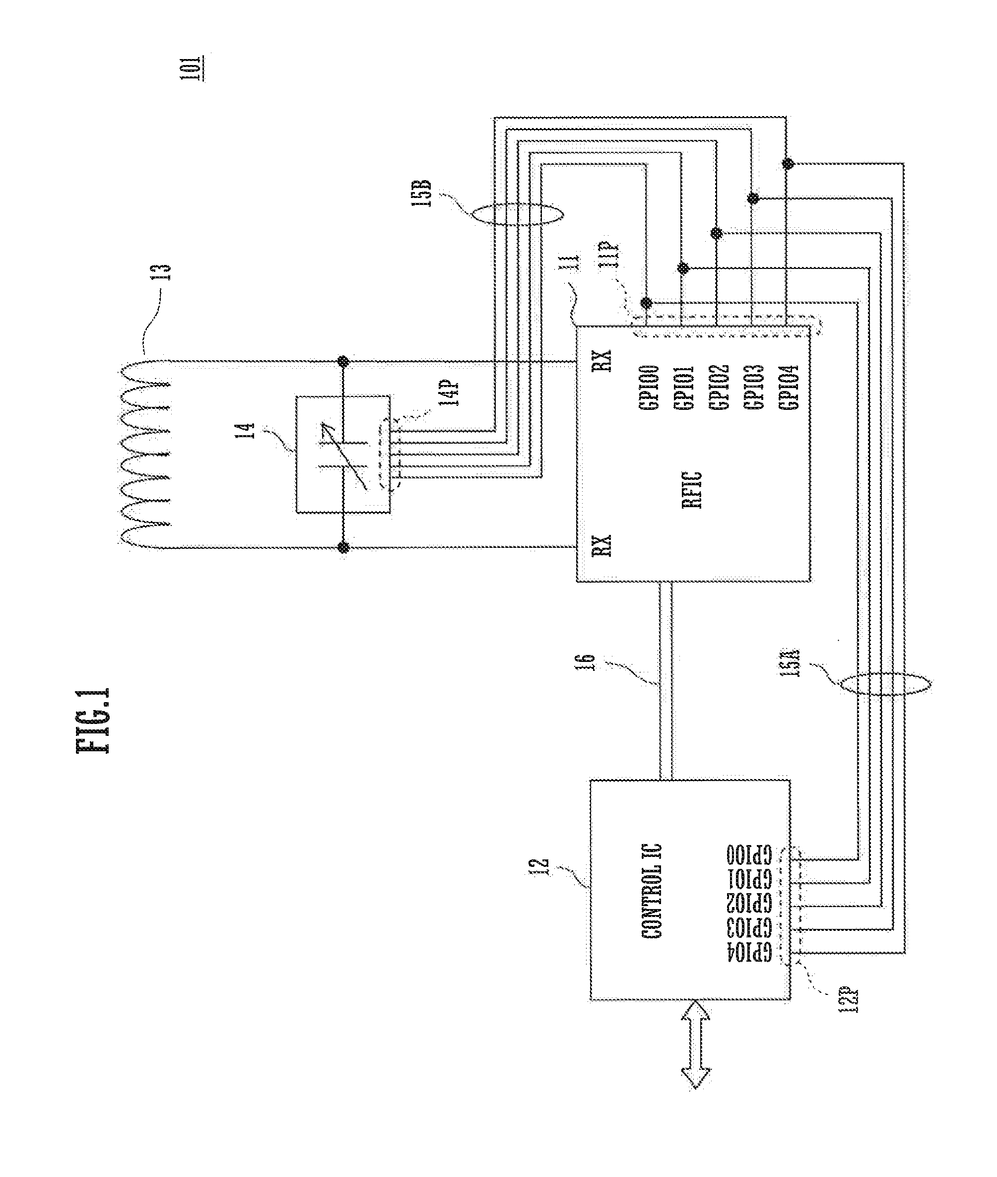
[0039]FIG. 1 is a circuit diagram of a communication circuit 101 according to a first preferred embodiment of the present invention. The communication circuit 101 is one example of an NFC module described above. The communication circuit 101 preferably includes an RFIC 11, a control IC 12, an antenna coil 13, and a variable capacitance element 14. The RFIC 11 includes IO terminals 11P for GPIO (General Purpose Input / Output). Similarly, the control IC 12 includes IO terminals 12P for GPIO.
[0040]The RFIC 11 is programmed and configured to perform modulation and demodulation between a baseband signal and a high-frequency signal. The control IC 12 may be called a host IC. The control IC controls the RFIC 11, and receives and transmits data including communication data.
[0041]The variable capacitance element 14 includes control terminals 14P. The variable capacitance element 14 includes a capacitance element with a capacitance value that is determined according to a control voltage (bias ...
second preferred embodiment
[0055]FIG. 6 is a circuit diagram of a communication circuit 102 according to a second preferred embodiment of the present invention. The communication circuit 102 is one example of the NFC module. The communication circuit 102 includes an RFIC 111, a control IC 12, an antenna coil 13, and a variable capacitance element 114. In this example, the RFIC 111 and the variable capacitance element 114 are provided within a single RFIC (variable-capacitance-element built-in RFIC) 110. The variable-capacitance-element built-in RFIC 110 preferably is a monolithic IC in which a circuit unit of the RFIC 111 and a circuit unit of the variable capacitance element 114 are provided on an Si substrate through a series of semiconductor fabrication. With this configuration, the number of the components is significantly reduced, wiring of the data transmission lines are greatly simplified to a large extent, and thus the size and the weight of the communication circuit are greatly reduced.
[0056]Further,...
third preferred embodiment
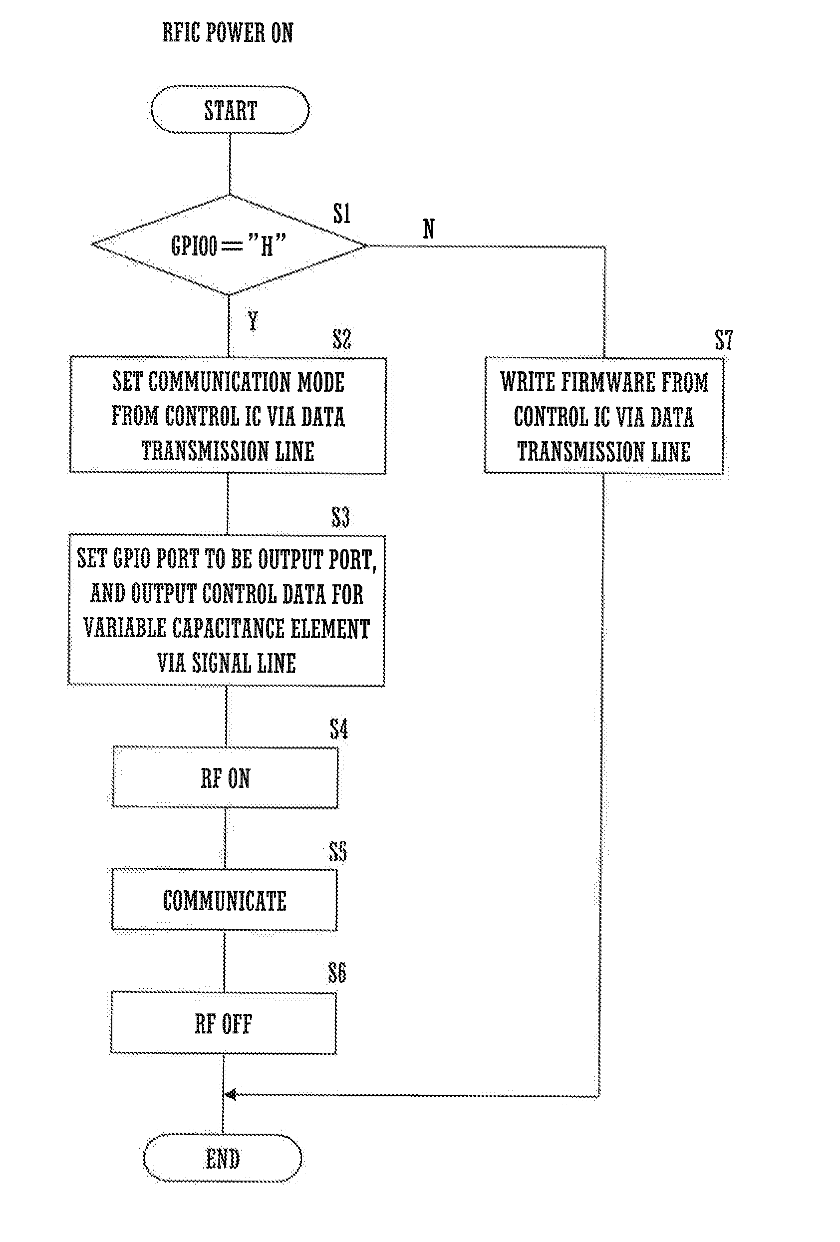
[0059]In a third preferred embodiment of the present invention, a processing of the RFIC (11 or 111) in the communication circuit described in one of the first preferred embodiment and the second preferred embodiment will be described. FIG. 8 is a flowchart of the processing. Upon turning the power of the RFIC on, the RFIC reads a state of GPIO0, which is one of the GPIO ports, and the processing branches according to its level. If the GPIO0 is high level, the RFIC receives data to set a communication protocol from the control IC via a data transmission line (see the data transmission lines 16 in FIG. 1), and sets the communication protocol (S1→S2). Then, the RFIC sets the GPIO port to be an “output port”, and outputs the control data for the variable capacitance element via the signal line (S3). With this, the capacitance value of the variable capacitance element is set to a value corresponding to this control data. For example, the capacitance value of the variable capacitance ele...
PUM
 Abstract
Description
Claims
Application Information
 - Generate Ideas
- Intellectual Property
- Life Sciences
- Materials
- Tech Scout
- Unparalleled Data Quality
- Higher Quality Content
- 60% Fewer Hallucinations
Browse by: Latest US Patents, China's latest patents, Technical Efficacy Thesaurus, Application Domain, Technology Topic, Popular Technical Reports.
© 2025 PatSnap. All rights reserved.Legal|Privacy policy|Modern Slavery Act Transparency Statement|Sitemap|About US| Contact US: help@patsnap.com