
Electronic component mounting method, electronic component placement machine, and electronic component mounting system

Inactive Publication Date: 2014-08-21
PANASONIC INTELLECTUAL PROPERTY MANAGEMENT CO LTD
View PDF5 Cites 13 Cited by
  • Summary
  • Abstract
  • Description
  • Claims
  • Application Information

AI Technical Summary

Benefits of technology

The present invention relates to a method of mounting electronic components on a substrate using a thermosetting resin. The invention is designed to prevent the resin from entering between the electrodes and bumps on the substrate, which can lead to poor electrical connection. By placing the electronic component on the substrate and dispensing the resin at the reinforcement position, the method ensures sufficient wetting of the electrodes during reflowing and ensures strong joining strength at the solder joints. Overall, the invention improves the mounting process of electronic components on substrates.

Problems solved by technology

When thermal stress generated by thermal cycling, or external force, is applied to a mounting structure comprising a substrate and electronic components obtained through the aforementioned mounting process, and if the electronic components are joined to the substrate via the bumps, the solder joints may lack sufficient strength.
Therefore, an additional heating for thermally curing the underfill material is required, which increases the number of processes required for mounting.
Moreover, the area where the underfill material adheres is large, and this is inconvenient when repairing the mounting structure.
Furthermore, when the substrate having solder joints reinforced with an underfill material is reflowed again, solder bridging is likely to occur at gaps caused in the underfill material.

Method used


Image

  • Electronic component mounting method, electronic component placement machine, and electronic component mounting system
  • Electronic component mounting method, electronic component placement machine, and electronic component mounting system
  • Electronic component mounting method, electronic component placement machine, and electronic component mounting system

Examples


example 1

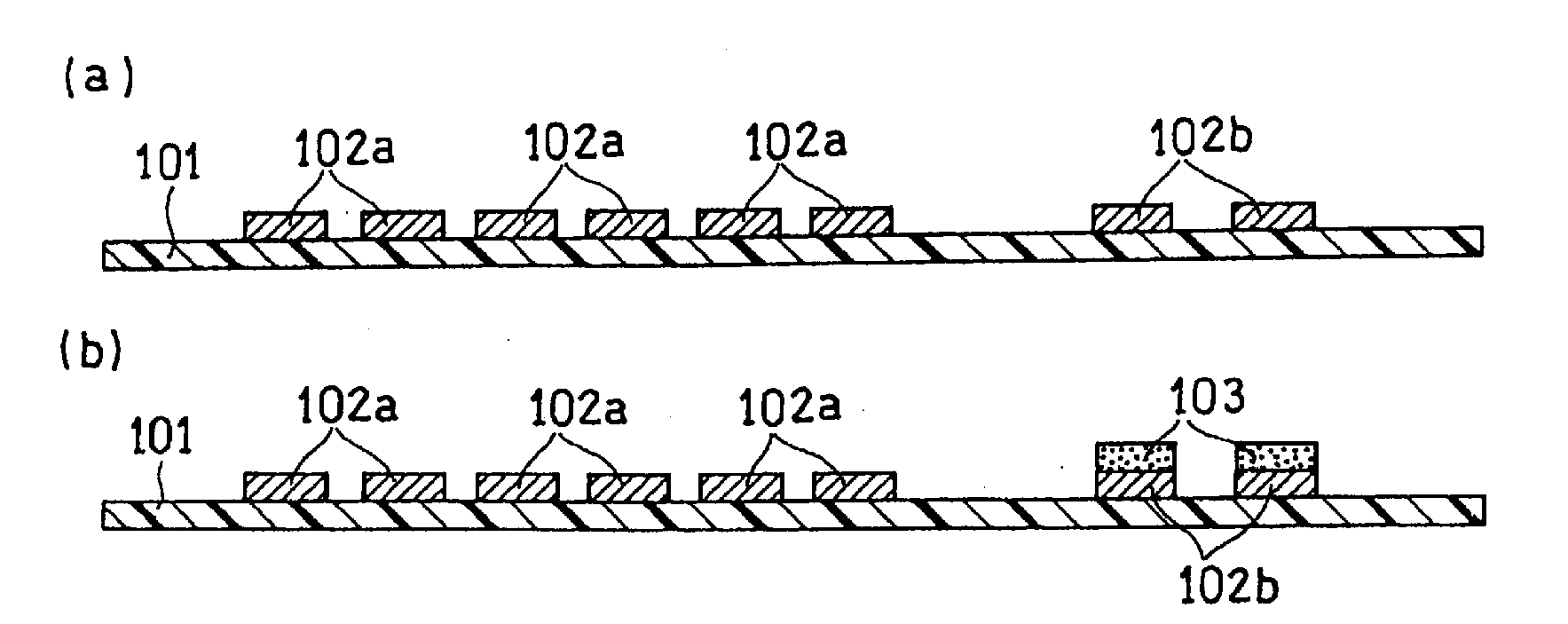
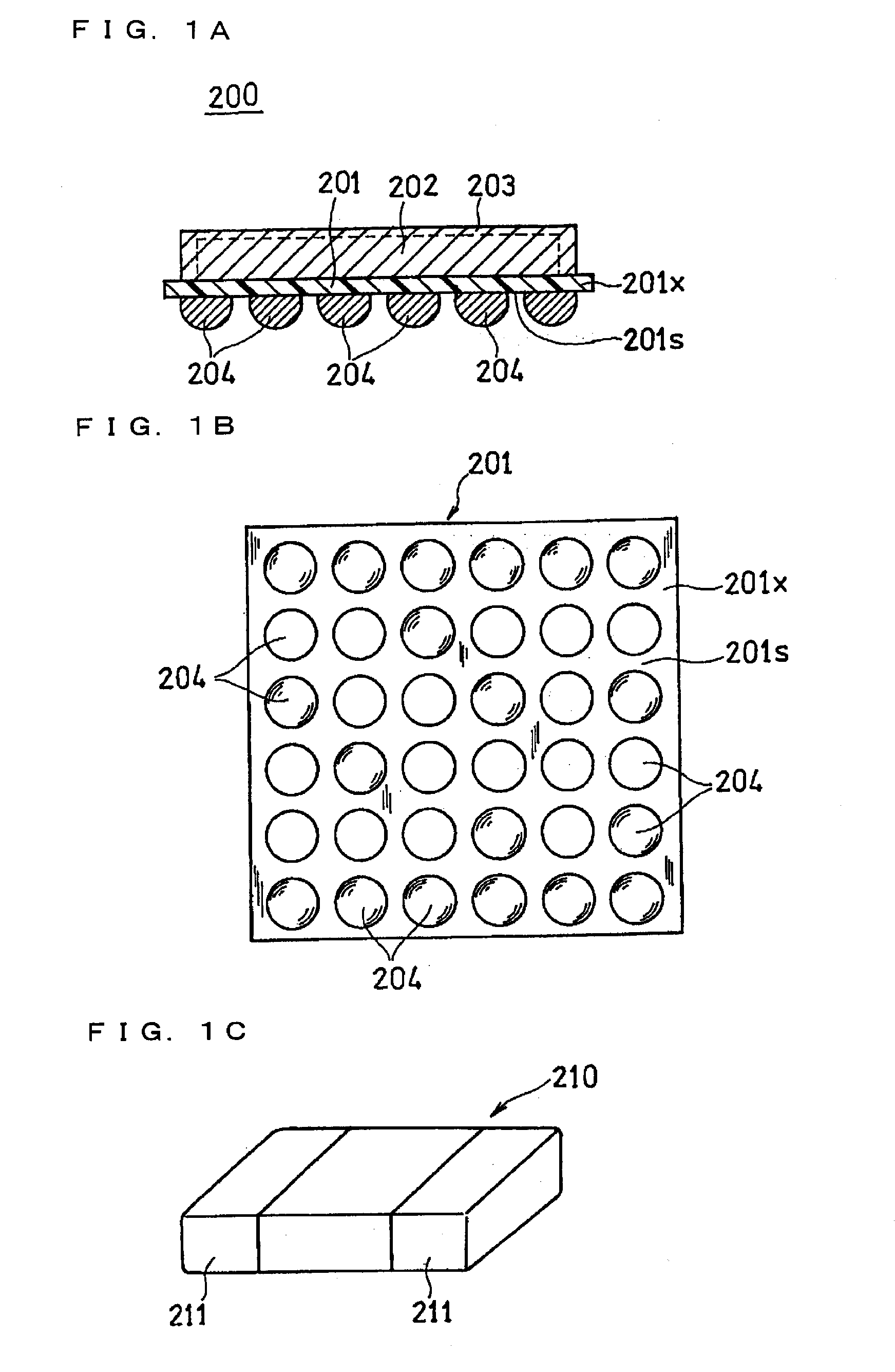
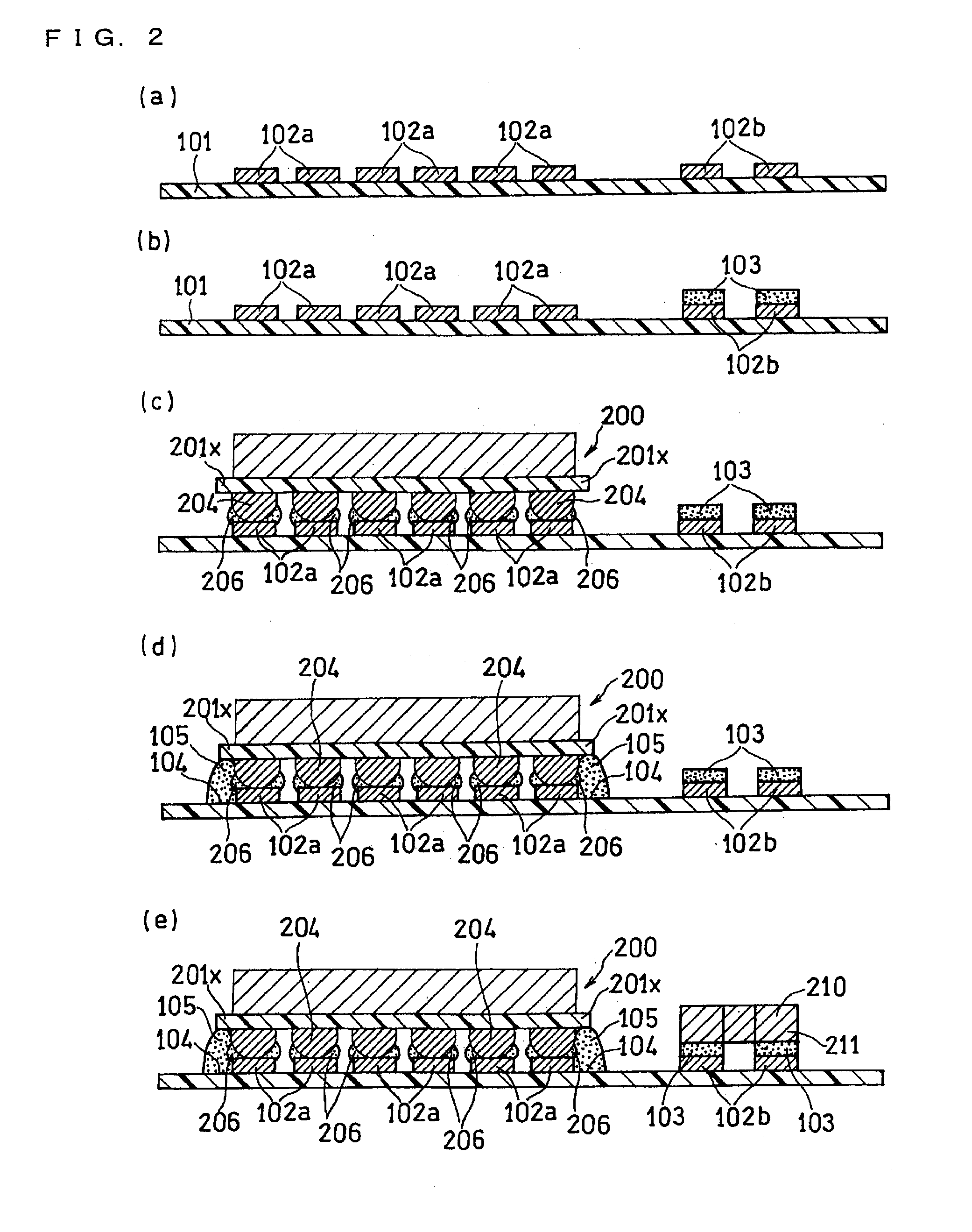
[0129]First, lands were formed on an FR4 substrate in a predetermined pattern, as first electrodes. A film of flux was formed on a transfer table by using a squeegee, and the film was transferred onto Sn—Ag—Cu solder bumps (melting point: approx. 220° C.) on a flip chip BGA package (1005 chip) used as a first electronic component. Thereafter, the electronic component was placed on the substrate such that the bumps landed on the lands. Next, a reinforcing resin was dispensed in a U-shaped dispensing pattern (FIG. 12(e)) onto two reinforcement positions set so as to include the four corners and vicinities of the peripheral edge portion of the electronic component. At that time, the reinforcing resin was brought into contact with the peripheral edge portion of the electronic component, and with the lands on the substrate and the bumps on the electronic component. Thereafter, the substrate with the electronic component placed thereon was heated at 240° C. to 250° C. in a reflow machine,...


PUM


Abstract

Disclosed is an electronic component mounting method including the steps of: providing a first electronic component having a principal surface provided with a plurality of bumps; providing a substrate having a plurality of first electrodes corresponding to the plurality of bumps; applying flux to the plurality of bumps; placing the first electronic component on the substrate such that the bumps land on the corresponding first electrodes via the flux; dispensing a thermosetting resin to at least one reinforcement position on the substrate with the first electronic component placed thereon, the at least one reinforcement position corresponding to a peripheral edge portion of the first electronic component; and heating the substrate with the first electronic component placed thereon, to melt the bumps and cure the thermosetting resin, followed by cooling, thereby to join the first electronic component to the substrate.

Description

TECHNICAL FIELD [0001]The present invention relates to a method and a machine for placing or mounting, on a substrate, an electronic component having a plurality of bumps.BACKGROUND ART [0002]Various electronic components are incorporated in electronic devices. These electronic components are joined at predetermined positions on a substrate having a plurality of electrodes and lead frames, and are incorporated as such as a mounting structure in the devices. With the advancement of miniaturization of electronic devices in recent years, the electronic components incorporated in the devices are being more and more miniaturized, thus causing increased use of small-sized electronic components such as flip chips and chip size packages (CSPs) to be place on a substrate.[0003]Electronic components such as flip chips and CSPs have a principal surface on which a plurality of terminals are regularly arranged in an array, and each terminal has a solder bump formed thereon. In mounting such an e...

Claims


Application Information

Patent Timeline
IPC IPC(8): H05K13/04
CPCH05K13/0465H05K3/3436H05K3/3442H05K3/3489H05K2201/10977H01L2924/19105H01L2224/11822H01L2224/81011H01L2224/7515H01L23/3114H01L23/3128H01L21/563H01L24/13H01L24/16H01L24/29H01L24/32H01L24/33H01L24/73H01L24/75H01L24/81H01L24/83H01L24/92H01L2224/16238H01L2224/32052H01L2224/32225H01L2224/75611H01L2224/81143H01L2224/81191H01L2224/81192H01L2224/8121H01L2224/81594H01L2224/81815H01L2224/83862H01L2224/9205H01L2224/97H01L2224/816H01L2224/83104H01L2224/33155H01L2224/75161H01L25/16H01L2224/2919H01L2224/73203H01L2224/9211H01L2924/351H01L2224/81024H01L2224/81986H01L2224/7901Y02P70/50H01L2224/81H01L2924/00014H01L2924/014H01L2924/00012H01L2224/83H01L2924/00
Inventor SAEKI, TSUBASAWADA, YOSHIYUKIMOTOMURA, KOJISAKAI, TADAHIKO
Owner PANASONIC INTELLECTUAL PROPERTY MANAGEMENT CO LTD
Learn More