Analog-to-digital converter and analog-to-digital conversion method
a converter and analog-to-digital technology, applied in the field of analog-to-digital converters and analog-to-digital conversion methods, can solve the problems of increasing development costs and capital investment, speed is further accelerated, and it is difficult to realize such a high-speed and highly accurate adc for communication purposes, etc., to achieve the effect of suppressing power consumption
- Summary
- Abstract
- Description
- Claims
- Application Information
AI Technical Summary
Benefits of technology
Problems solved by technology
Method used
Image

Examples
first exemplary embodiment
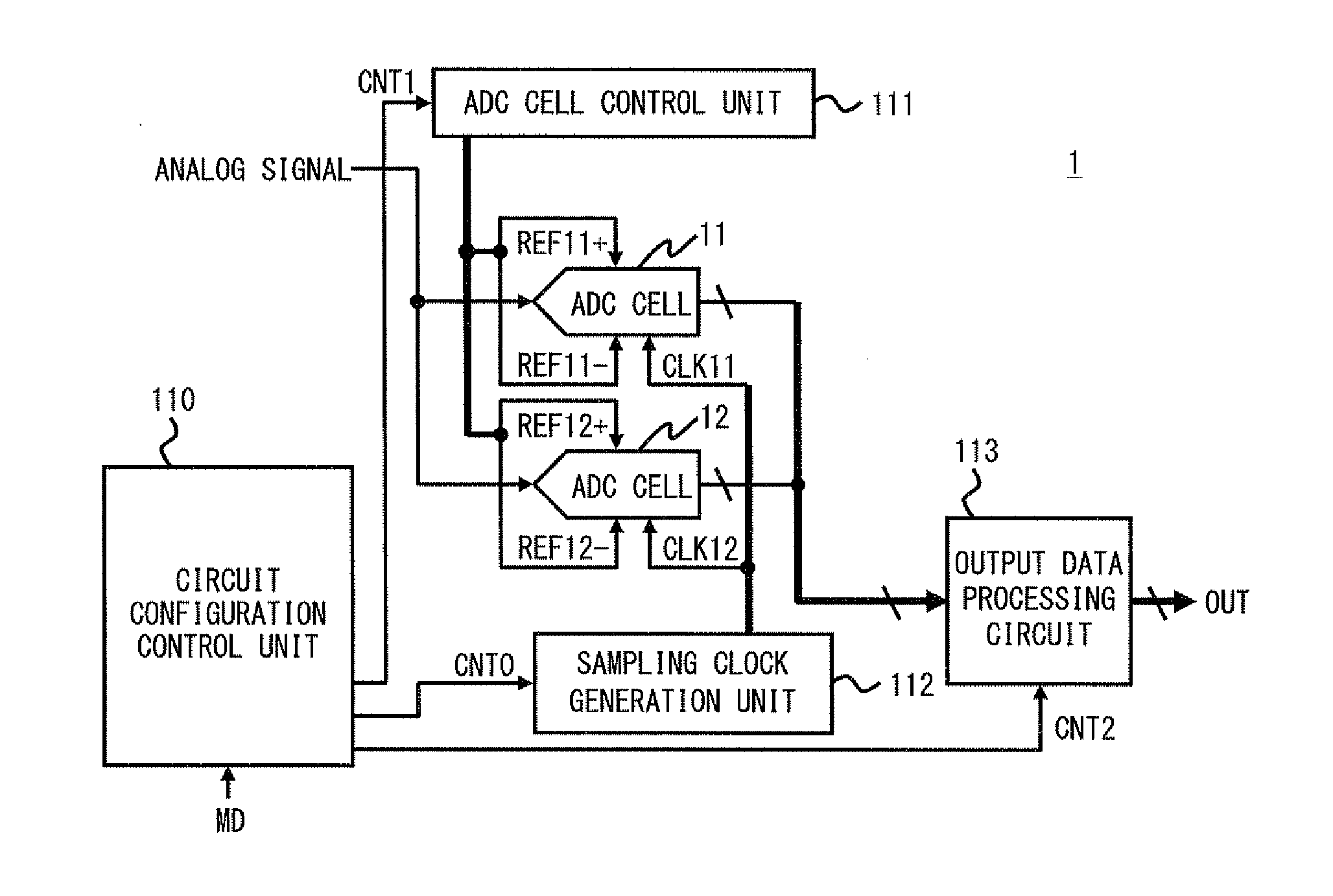
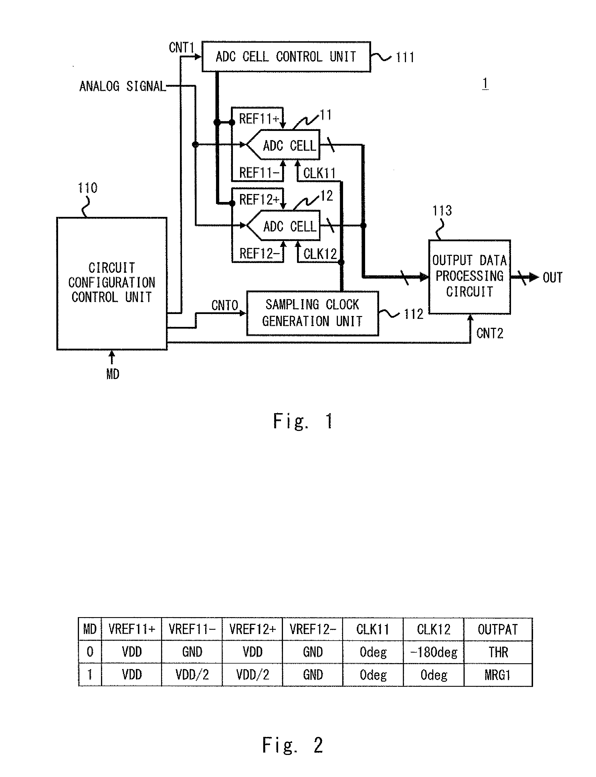
[0050]Hereinafter, exemplary embodiments of the present invention shall be explained with reference to the drawings. FIG. 1 is a block diagram of an entire analog-to-digital converter 1 of the present invention. As shown in FIG. 1, the analog-to-digital converter 1 according to the first exemplary embodiment includes analog-to-digital conversion cells (hereinafter referred to as ADC cells) 11 and 12, a circuit configuration control unit 110, an ADC cell control unit 111, a sampling clock generation unit 112, and an output data processing circuit 113.
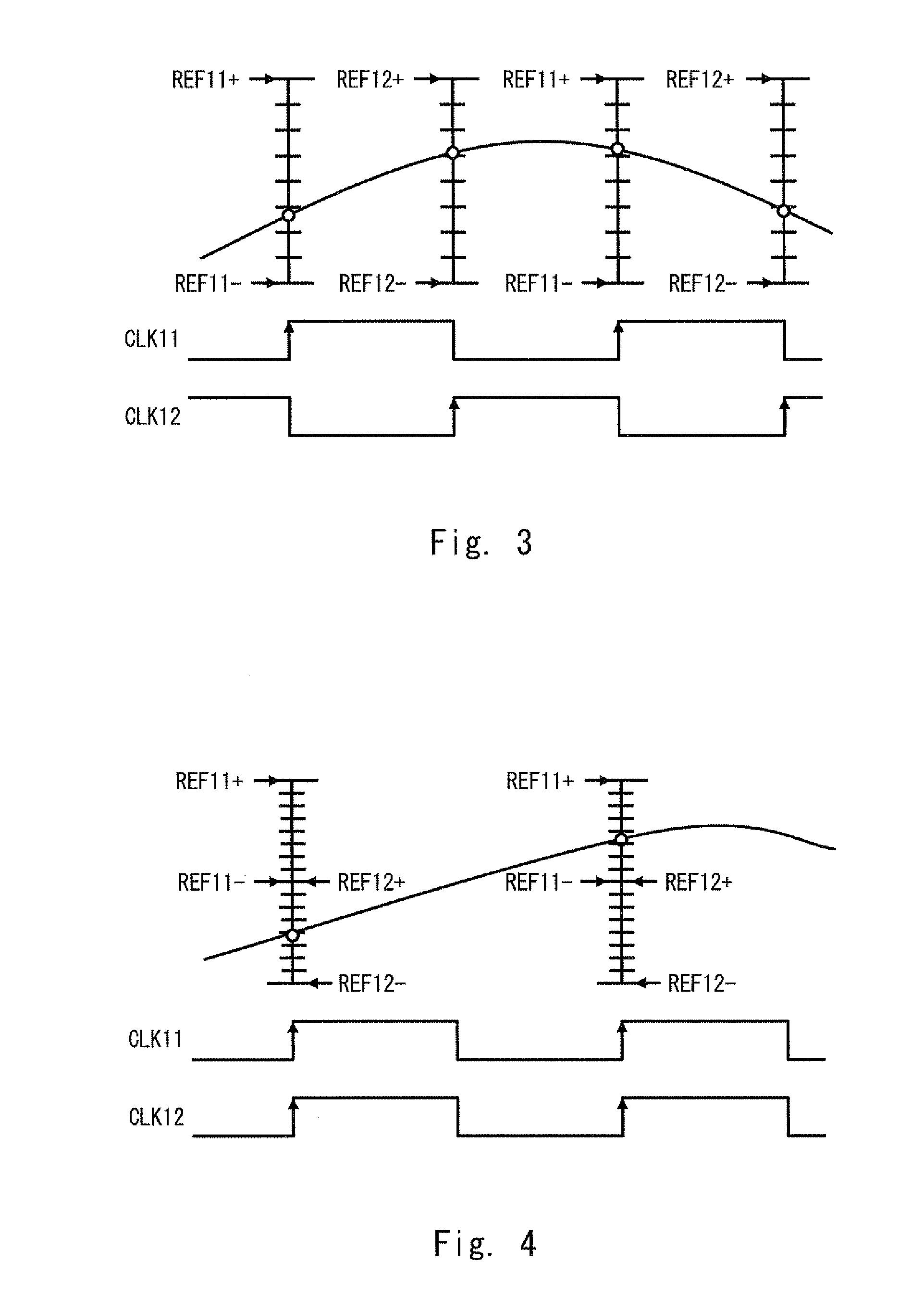
[0051]Note that the first exemplary embodiment explains an example in which the analog-to-digital converter 1 has, as operation modes, a first mode for performing high-speed and low accuracy conversion processing and a second mode for performing low-speed and high accuracy conversion processing. Moreover, in the following explanation, conversion accuracy indicates the size of the quantization step voltage. That is, a small quantization s...
second exemplary embodiment
[0071]FIG. 6 is a block diagram of an analog-to-digital converter 2 according to a second exemplary embodiment. As shown in FIG. 6, an analog-to-digital converter 2 according to the second exemplary embodiment increases the number of ADC cells in the analog-to-digital converter 1 according to the first exemplary embodiment to three or more. In the example shown in FIG. 6, n (n is an integer indicating the number of ADC cells) ADC cells are shown.
[0072]In the analog-to-digital converter 2 according to the second exemplary embodiment, it is possible to support more communication schemes than are supported by the analog-to-digital converter 1 according to the first exemplary embodiment by including more ADC cells than are in the analog-to-digital converter 1. Therefore, in the second exemplary embodiment, a configuration table that defines usage of the ADC cells 11 to 1n shall be explained in detail. Note that basic functions of the blocks in the analog-to-digital converter 2 according...
third exemplary embodiment
[0088]FIG. 12 is a block diagram of an analog-to-digital converter 3 according to a third exemplary embodiment. As shown in FIG. 12, the analog-to-digital converter 3 further includes, in addition to the circuits in the analog-to-digital converter 2 according to the second exemplary embodiment, preprocessing circuits 11p to 1np. Moreover, the analog-to-digital converter 3 supplies maximum reference voltages and minimum reference voltages, which are the same voltages respectively, to the ADC cells 11 to 1n. Therefore, in FIG. 12, a maximum reference voltage REF+ and a minimum reference voltage REF− are supplied to all of the ADC cells 11 to 1n. Thus, as a variation range of an analog signal which will be input to the analog-to-digital converter 3, a range larger than the input voltage ranges of the respective ADC cells 11 to 1n, that is, a range larger than a range between the maximum reference voltage REF+ and the minimum reference voltage REF− can be supported. The method shall be ...
PUM
 Abstract
Description
Claims
Application Information
 - R&D
- Intellectual Property
- Life Sciences
- Materials
- Tech Scout
- Unparalleled Data Quality
- Higher Quality Content
- 60% Fewer Hallucinations
Browse by: Latest US Patents, China's latest patents, Technical Efficacy Thesaurus, Application Domain, Technology Topic, Popular Technical Reports.
© 2025 PatSnap. All rights reserved.Legal|Privacy policy|Modern Slavery Act Transparency Statement|Sitemap|About US| Contact US: help@patsnap.com