Imaging device

Active Publication Date: 2014-08-28
SEMICON ENERGY LAB CO LTD
View PDF5 Cites 12 Cited by
  • Summary
  • Abstract
  • Description
  • Claims
  • Application Information

AI Technical Summary

Benefits of technology

[0020]According to one embodiment of the present invention, an imaging device which is highly stable to irradiation with radiations such as X-rays can be provided. An imaging device having a structure which can inhibit a de

Problems solved by technology

Such a phenomenon can occur by a slight amount of radiation which penetrates a scintillat

Method used


Image

  • Imaging device
  • Imaging device
  • Imaging device

Examples


embodiment 1

[0061]In this embodiment, an imaging device using radiations such as X-rays, which is one embodiment of the present invention, is described with reference to the drawings.

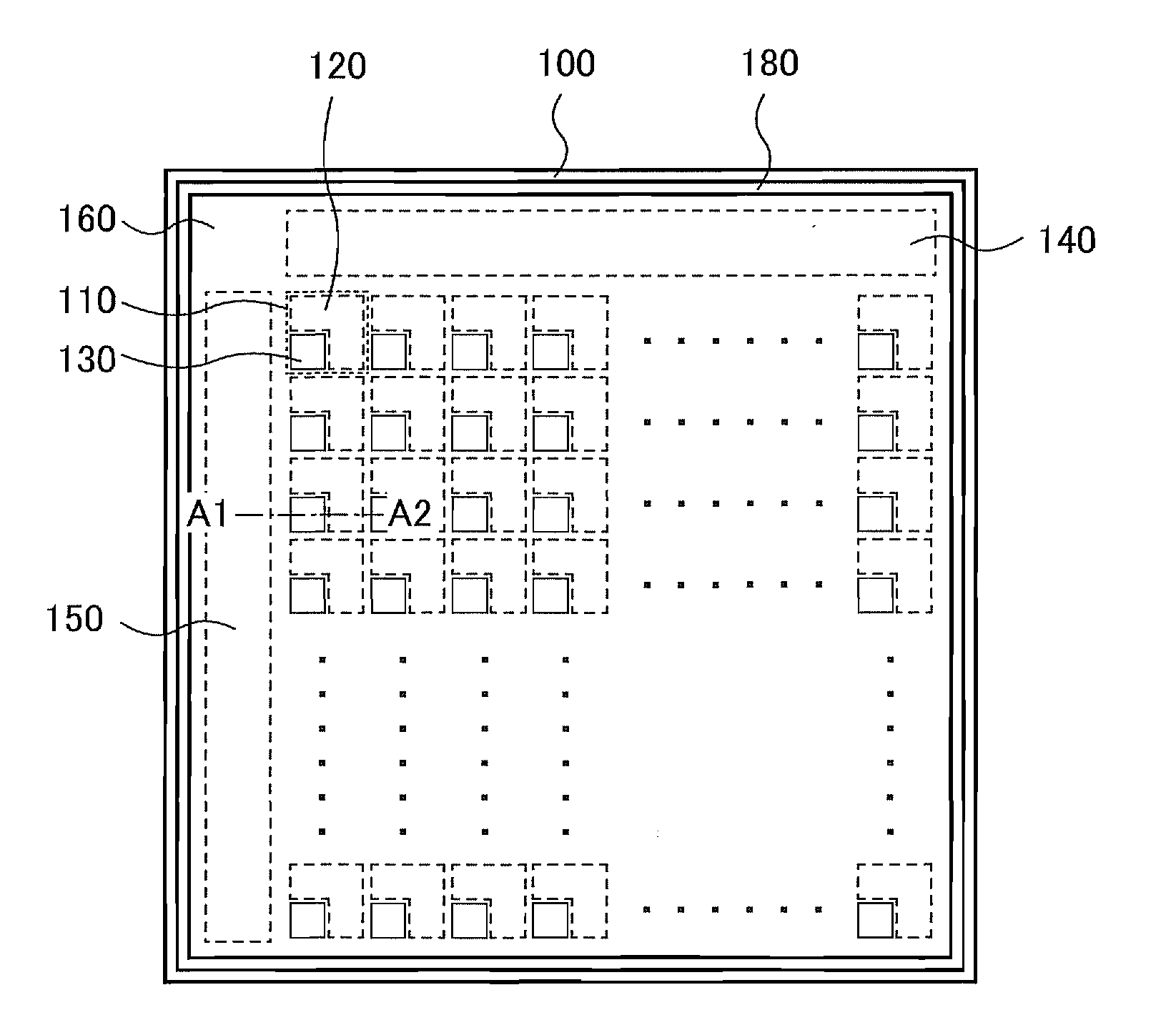
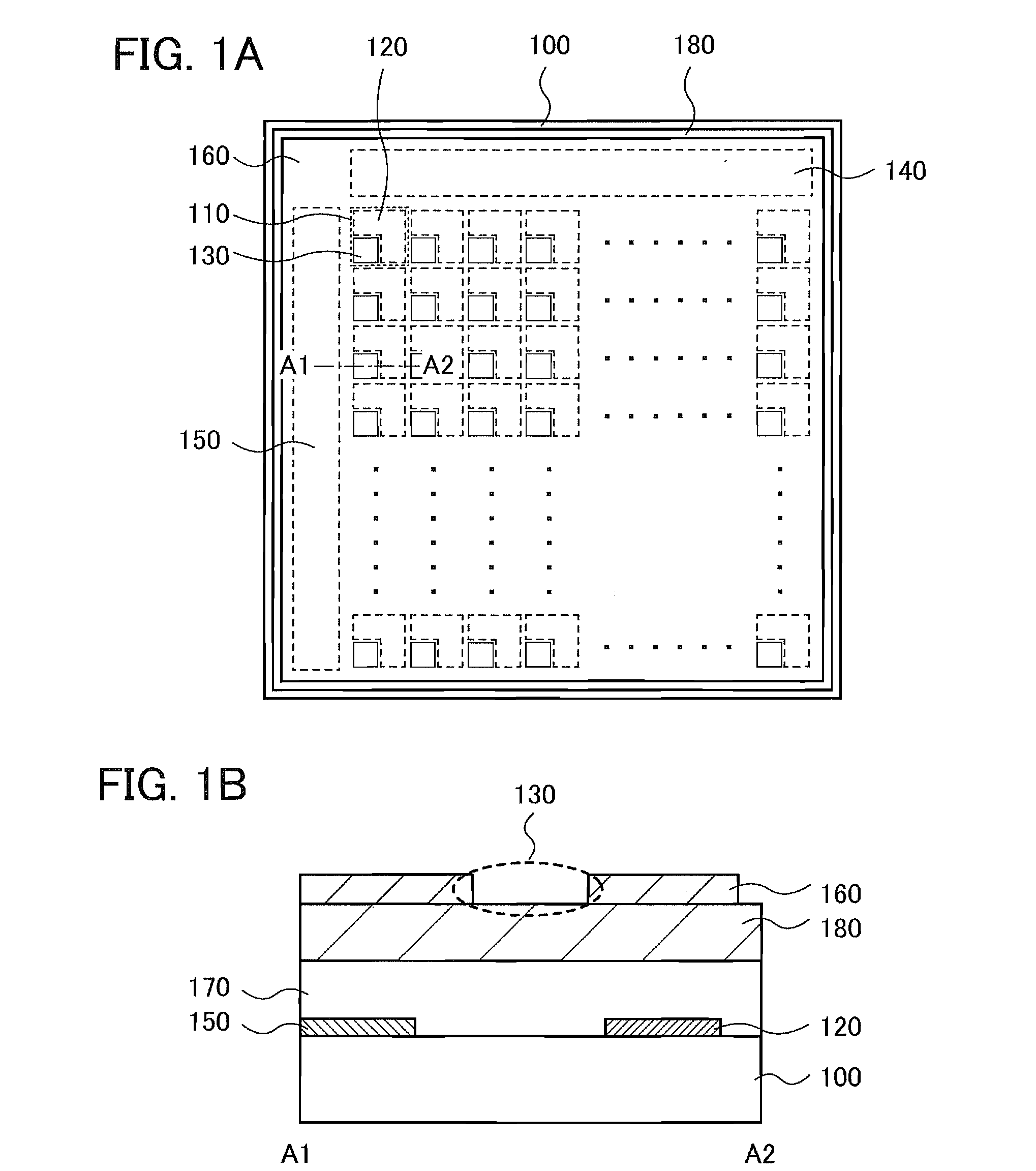
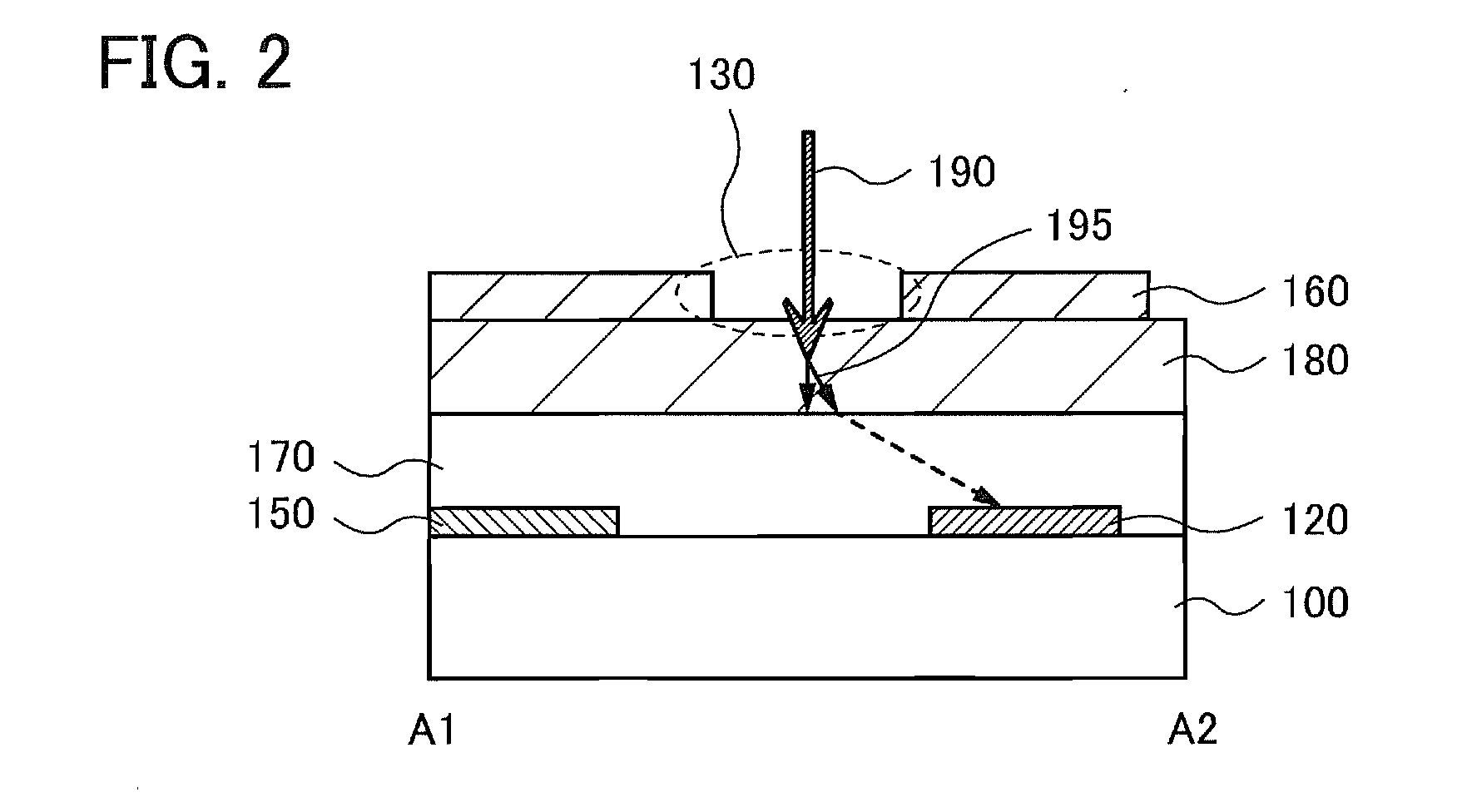
[0062]FIG. 1A is a top view of an imaging device of one embodiment of the present invention, and FIG. 1B is a cross-sectional view taken along dotted line A1-A2 in the top view. Note that for simplification of the drawing, some components are not illustrated in FIG. 1A.

[0063]The imaging device of one embodiment of the present invention includes pixel circuits 110 arranged in a matrix over a substrate 100, a first circuit 140 and a second circuit 150 for driving the pixel circuits, an interlayer insulating film 170 and a scintillator 180 which are formed over the pixel circuits 110, the first circuit 140, and the second circuit 150, and a shielding layer 160 overlapping the scintillator.

[0064]In FIG. 1A, the circuits for driving the pixel circuits 110 are the first circuit 140 and the second circuit 150 and are posi...

embodiment 2

[0091]In this embodiment, a circuit which can be used as the pixel circuit in Embodiment 1 is described.

[0092]FIG. 8A shows an example of a circuit which can be used as the pixel circuit 110. A circuit 200 includes a photodiode 220, a first transistor 201, a second transistor 202, and a third transistor 203.

[0093]An anode of the photodiode 220 is electrically connected to a first wiring 211 (RS); a cathode of the photodiode 220 is electrically connected to one of a source and a drain of the first transistor 201; the other of the source and the drain of the first transistor 201 is electrically connected to a wiring 205 (FD); a gate of the first transistor 201 is electrically connected to a second wiring 212 (TX); one of a source and a drain of the second transistor 202 is electrically connected to a fourth wiring 214 (GND); the other of the source and the drain of the second transistor 202 is electrically connected to one of a source and a drain of the third transistor 203; a gate of...

embodiment 3

[0167]In this embodiment, an example of a driving method of the pixel circuit described in Embodiment 2 is described.

[0168]As described in Embodiment 2, the operation of the pixel circuit is repetition of the reset operation, the accumulation operation, and the selection operation. In the imaging device using radiations such as X-rays, radiation exposure time is preferably as short as possible in consideration of influence of X-rays on the living body. To achieve irradiating with radiation and imaging in short time, it is necessary to perform the reset operation, the accumulation operation, and the selection operation of all the pixel circuits at high speed.

[0169]Thus, a driving method using a global shutter system illustrated in a timing chart in FIG. 16A is preferably used for imaging. Note that FIG. 16A shows operations of the imaging device in which a plurality of pixel circuits is arranged in a matrix and the pixel circuits are the circuits 200 in FIG. 8A, specifically, operati...


PUM


Abstract

An imaging device which is highly stable to irradiation with radiations such as X-rays and can inhibit a decrease in electrical characteristics is provided. The imaging device obtains an image using radiations such as X-rays and includes pixel circuits which are arranged in a matrix and which a scintillator overlaps. Each of the pixel circuits includes a switching transistor whose off-state current is extremely low and a light-receiving element. A shielding layer formed using a metal material and the like overlaps the transistor and the light-receiving element. With the structure, an imaging device which is highly stable to irradiation with radiations such as X-rays and can inhibit a decrease in electrical characteristics can be provided.

Description

TECHNICAL FIELD[0001]The present invention relates to an object, a method, or a manufacturing method. In addition, the present invention relates to a process, a machine, manufacture, or a composition of matter. In particular, the present invention relates to, for example, a semiconductor device, a display device, a light-emitting device, a power storage device, a driving method thereof, or a manufacturing method thereof. In particular, the present invention relates to an imaging device including a scintillator.BACKGROUND ART[0002]In medical practice, a medical diagnostic imaging device using a photographic technique has been in wide use. With the medical diagnostic imaging device, a specific portion (e.g., bone or lungs) of a patient is irradiated with X-rays, an X-ray film is exposed to X-rays passing through the specific portion, and the X-ray film is developed to visualize a state inside the specific portion.[0003]Since the method using X-ray films needs a storage space for the X...

Claims


Application Information

Patent Timeline
IPC IPC(8): G01T1/20
CPCG01T1/2006G01T1/2019G01T1/20184G01T1/20185
Inventor YAMAZAKI, SHUNPEIAKIMOTO, KENGOTAKAHASHI, HIRONOBUKANEMURA, HIROSHIMIYANAGA, AKIHARU
Owner SEMICON ENERGY LAB CO LTD
Why Eureka
Try Eureka