

Display device and electronic device
a display device and electronic technology, applied in the direction of semiconductor devices, instruments, optics, etc., can solve the problems of high probability of electrostatic breakdown of the transistor, high probability of the wiring and the like connected to the transistor during the manufacturing process, and high probability of the manufacturing yield of the display device, so as to reduce the probability of electrostatic breakdown
Active Publication Date: 2014-08-28
SEMICON ENERGY LAB CO LTD
View PDF5 Cites 21 Cited by
- Summary
- Abstract
- Description
- Claims
- Application Information
AI Technical Summary
Benefits of technology
The present invention seeks to provide a display device with a novel structure that can reduce electrostatic breakdowns, improve reliability, reduce adverse effects of static electricity, reduce fluctuation or deterioration of transistor characteristics, inhibit normally-on of a transistor, increase manufacturing yield of transistors, and discharge electric charges accumulated in a pixel electrode and wiring, thus enabling normal display.
Problems solved by technology
That is, the transistor during the manufacturing process and a wiring and the like connected to the transistor are highly likely to be broken by static electricity or overcurrent which can be generated in the manufacturing process of the transistor.
Thus, there is a problem in that the manufacturing yield of display devices is very low when the display devices are manufactured in the state in which transistors and wirings and the like connected to the transistors are highly likely to be broken by static electricity or overcurrent which can be generated in a manufacturing process of the transistors.
Method used
View moreImage
Smart ImageViewing Examples

Examples
embodiment 1 (
1. Embodiment 1 (Basic structure of display device);
embodiment 2 (
2. Embodiment 2 (Method for manufacturing display device);
embodiment 3 (
3. Embodiment 3 (Modification example of display device);
Login to View More PUM
 Abstract
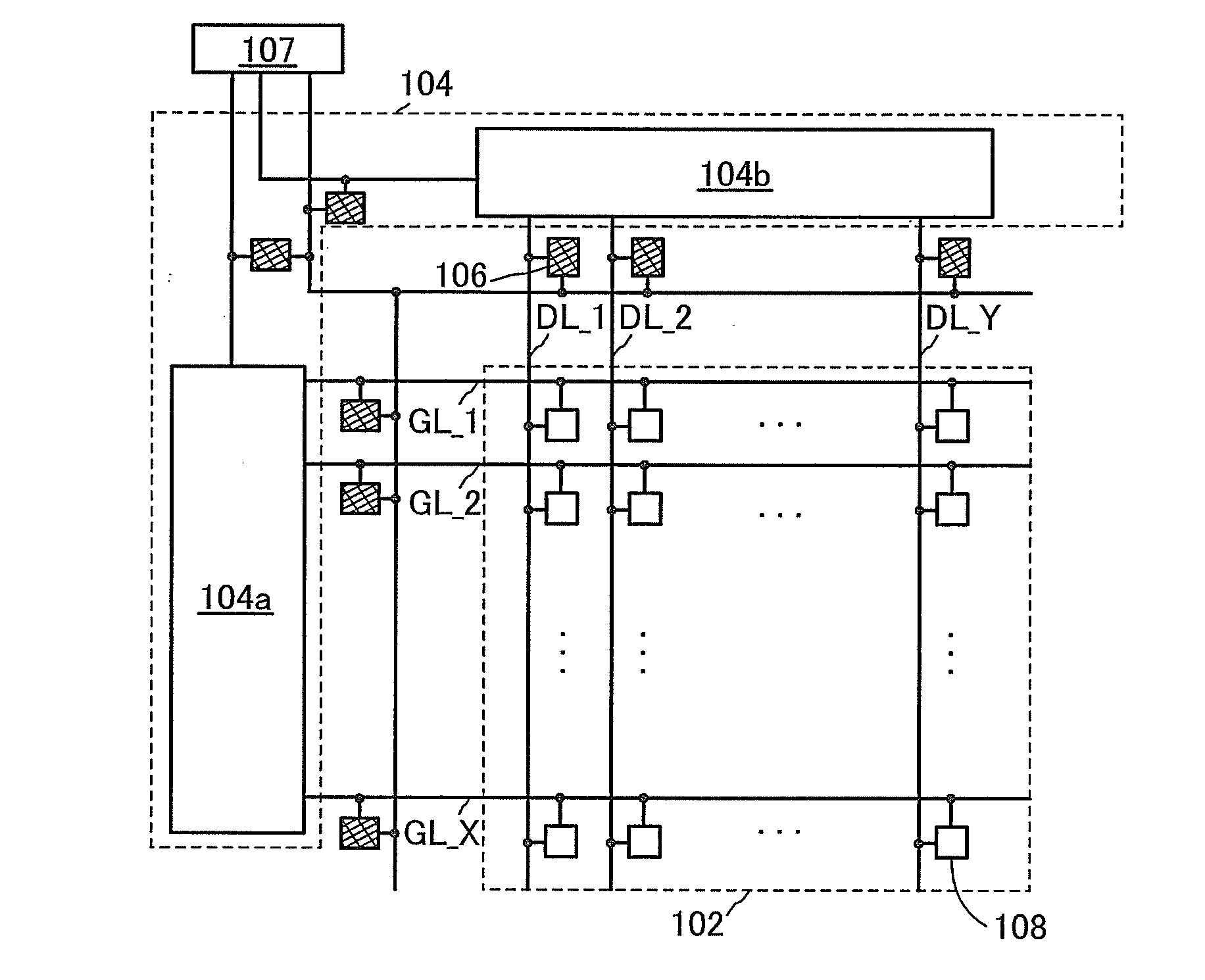
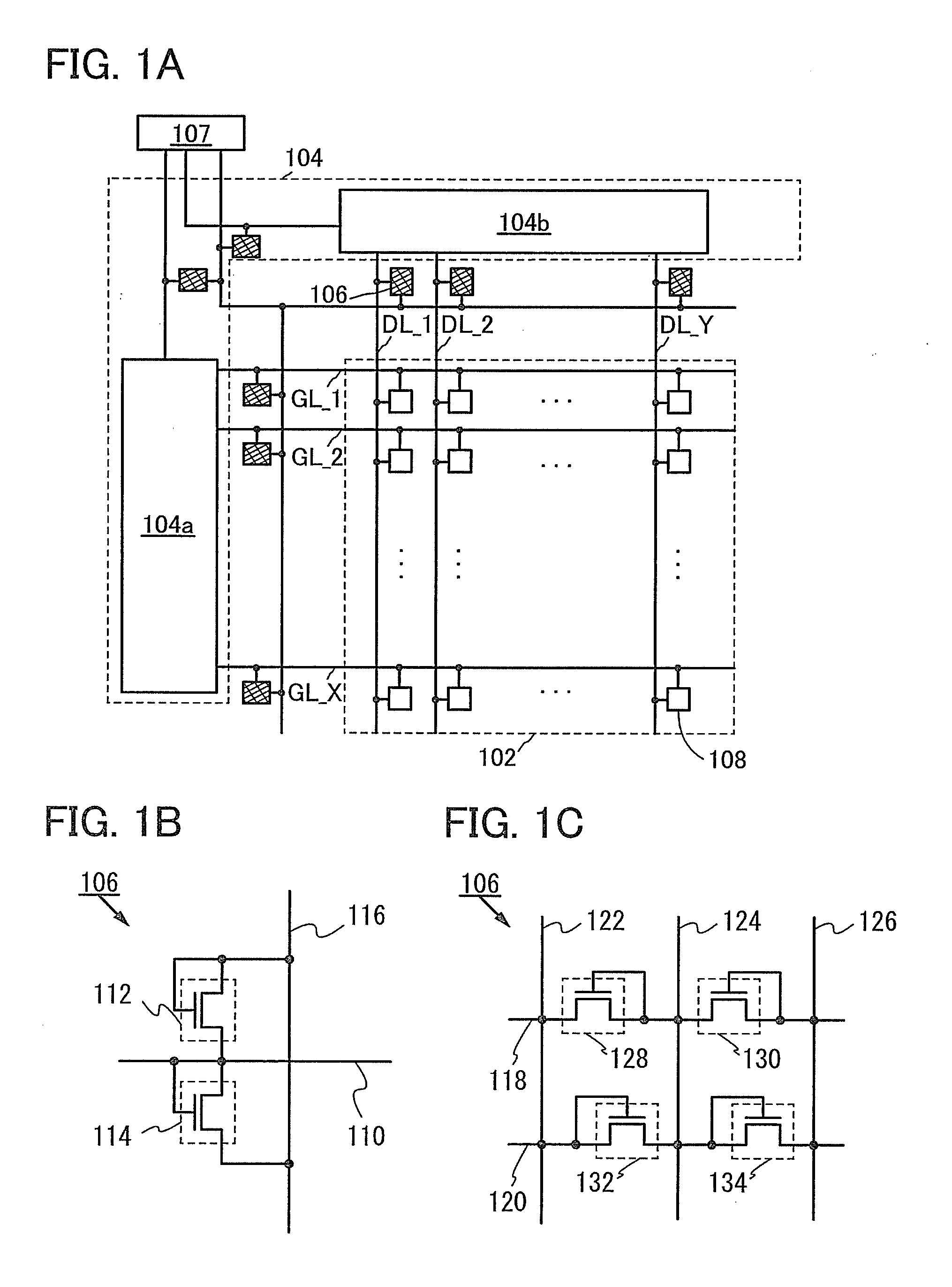
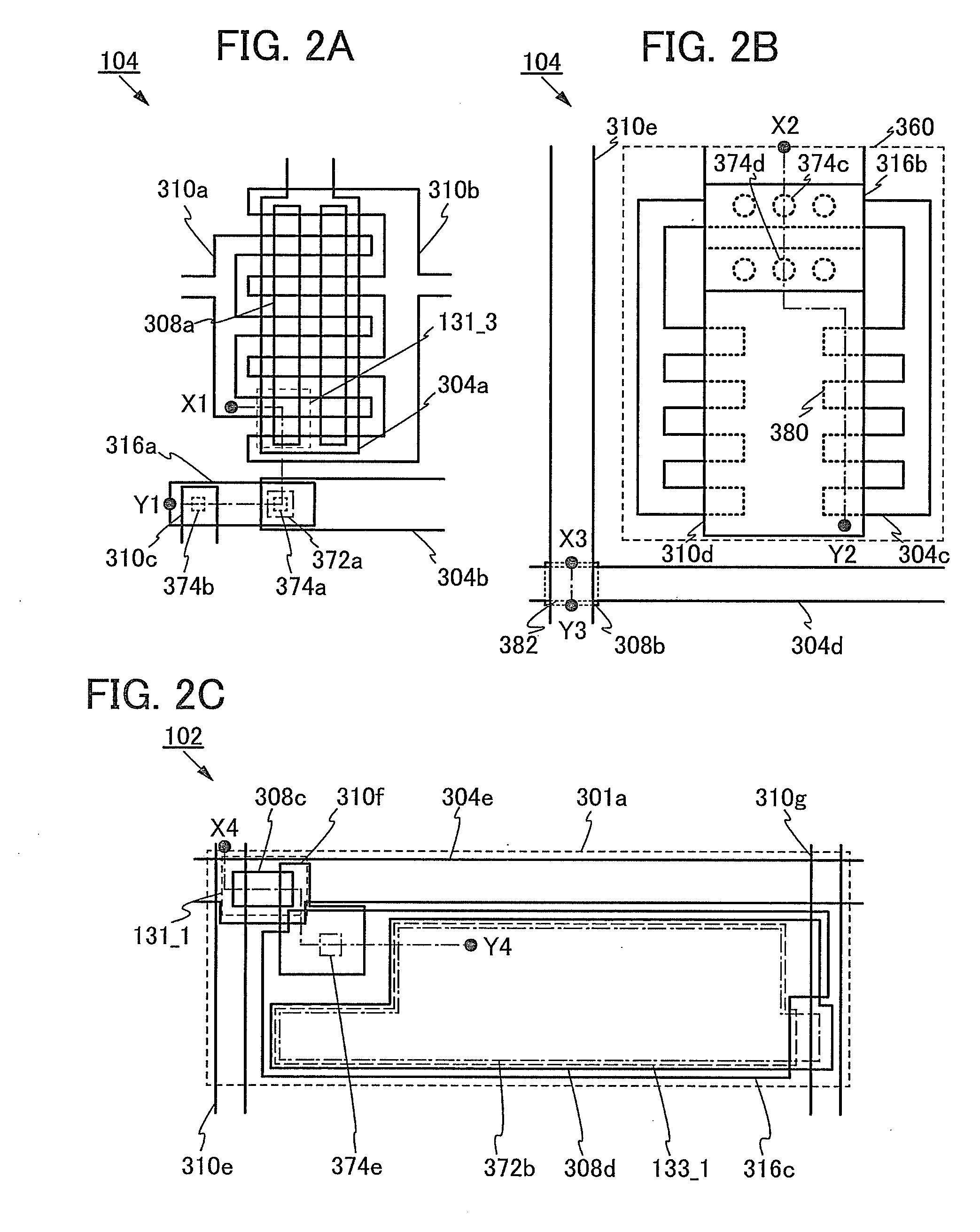
Transistors each include a gate electrode, a gate insulating layer over the gate electrode, an oxide semiconductor layer over the gate insulating layer, and a source electrode and a drain electrode over the oxide semiconductor layer. A driver circuit portion includes first to third wirings formed in the same step as the gate electrode, fourth to sixth wirings formed in the same step as the source electrode and the drain electrode, a seventh wiring formed in the same step as a pixel electrode, a first region where the second wiring intersects with the fifth wiring, and a second region where the third wiring intersects with the sixth wiring. The first wiring is connected to the fourth wiring through the seventh wiring. A distance between the wirings in the second region is longer than that in the first region.
Description
TECHNICAL FIELD[0001]The present invention relates to an object, a method, a method for producing an object, a process, a machine, manufacture, or a composition of matter. In particular, the present invention relates to a semiconductor device, a display device, a light-emitting device, an electronic device, a driving method thereof, or a manufacturing method thereof. In particular, the present invention relates to a semiconductor device, a display device, an electronic device or a light-emitting device each including an oxide semiconductor.[0002]Note that the term “display device” means a device having a display element. Note that the display device can also include, for example, a driver circuit for driving the plurality of pixels in some cases. The display device also includes a control circuit, a power supply circuit, a signal generation circuit, and the like which are arranged on another substrate, in some cases.BACKGROUND ART[0003]For display devices typified by liquid crystal ...
Claims
Login to View More Application Information
Patent Timeline
 IPC IPC(8): G02F1/1362
CPCG02F1/136286G02F1/136204H01L27/1225H01L27/124H01L29/66
InventorSHISHIDO, HIDEAKIMIYAKE, HIROYUKIINOUE, SEIKOTOYOTAKA, KOUHEIKUSUNOKI, KOJI
OwnerSEMICON ENERGY LAB CO LTD