Semiconductor device having deep wells and fabrication method thereof

Inactive Publication Date: 2014-09-04
DONGBU HITEK CO LTD
View PDF2 Cites 6 Cited by
  • Summary
  • Abstract
  • Description
  • Claims
  • Application Information

AI Technical Summary

Benefits of technology

[0011]Embodiments of the subject invention provide a deep well of a semiconductor device and a method of fabricating the same that simplifies processes by using a small number of masks i

Problems solved by technology

Thus, there are limitations, in that processes become complex and

Method used


Image

  • Semiconductor device having deep wells and fabrication method thereof
  • Semiconductor device having deep wells and fabrication method thereof
  • Semiconductor device having deep wells and fabrication method thereof

Examples


Example

[0020]Reference will now be made in detail to the embodiments of the present disclosure, examples of which are illustrated in the accompanying drawings.

[0021]When the terms “on” or “over” are used herein, when referring to layers, regions, patterns, or structures, it is understood that the layer, region, pattern, or structure can be directly on another layer or structure, or intervening layers, regions, patterns, or structures may also be present. When the terms “under” or “below” are used herein, when referring to layers, regions, patterns, or structures, it is understood that the layer, region, pattern, or structure can be directly under the other layer or structure, or intervening layers, regions, patterns, or structures may also be present.

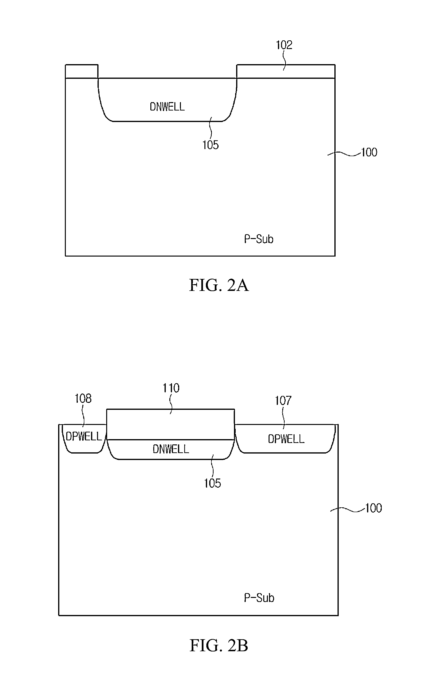
[0022]FIGS. 3A to 3D are cross-sectional views of a method of forming a deep well of a semiconductor device according to an embodiment of the subject invention.

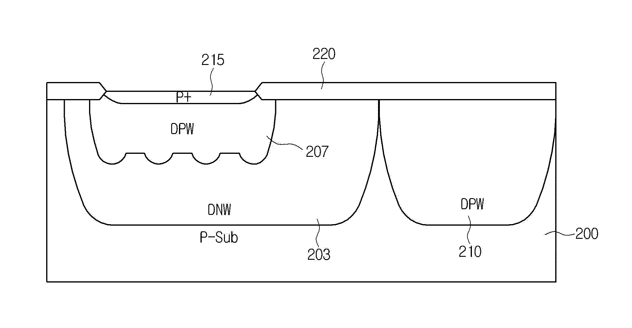
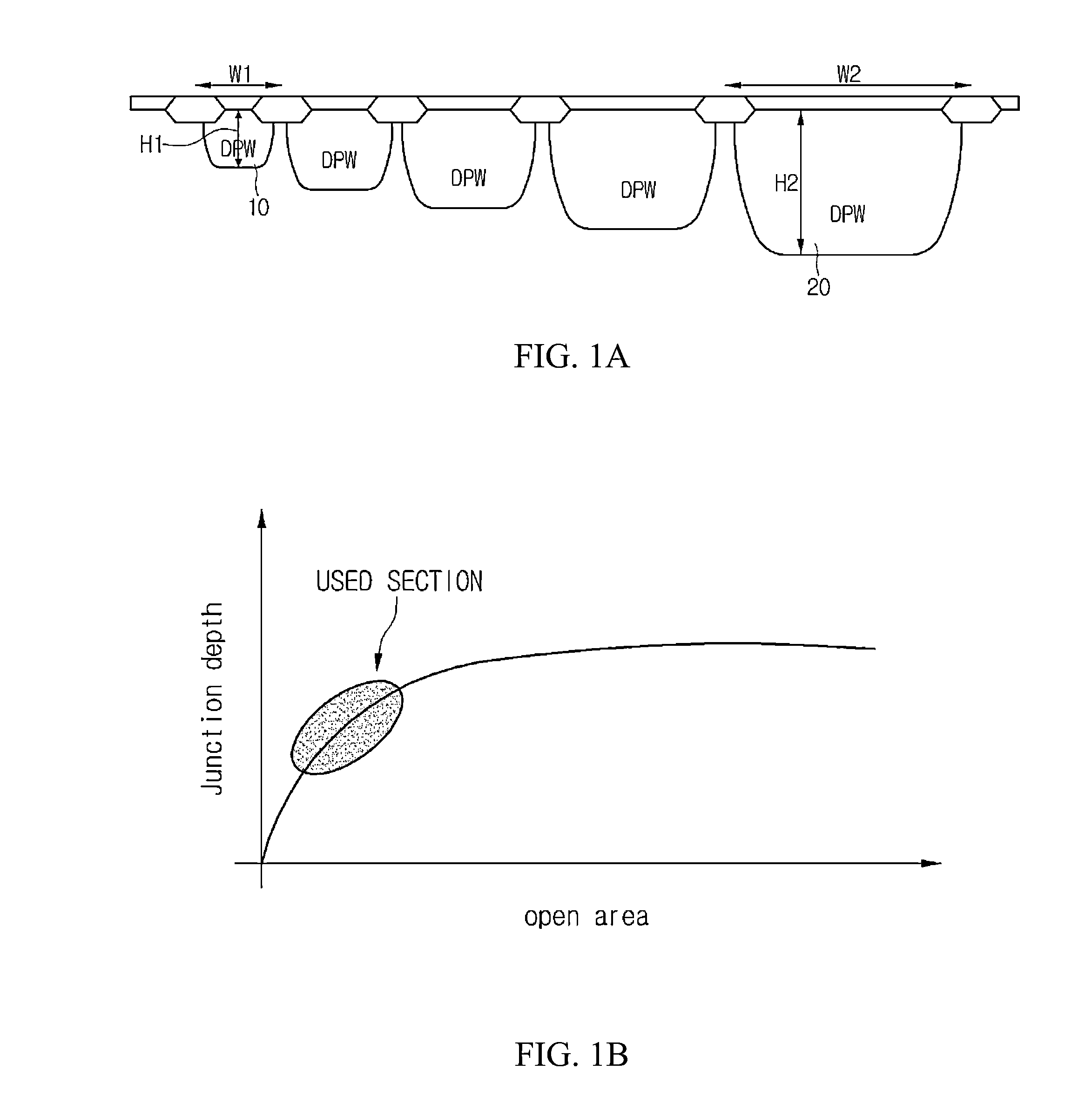
[0023]Referring to FIG. 3A, an insulating film 202 can be disposed on a P-doped sem...


PUM


Abstract

Semiconductor devices and methods of fabricating the same are provided. An insulating film can be disposed on a semiconductor substrate, and insulating film patterns can be formed opening a plurality of areas with predetermined widths by patterning the insulating film. A plurality of ion implantation areas having a first conductivity type can be formed by implanting impurities into the plurality of open areas, and an oxide film pattern can be formed on each of the ion implantation areas. The insulating film patterns can be removed, and ion implantation areas having a second conductivity type can be formed by implanting impurities using the oxide film pattern as a mask. The semiconductor substrate can be annealed at a high temperature to form deep wells.

Description

CROSS-REFERENCE TO RELATED APPLICATION[0001]This application claims the benefit under 35 U.S.C. §119 of Korean Patent Application No. 10-2013-0023047, filed Mar. 4, 2013, which is hereby incorporated by reference in its entirety.BACKGROUND[0002]A high-voltage semiconductor device used for, e.g., an LCD driver IC (LDI), a PDP driver IC, a flash memory, or EEPROM, needs to have high junction breakdown voltage. To this end, the high-voltage semiconductor device may be formed in a deep well with low doping distribution.[0003]The well used for the high-voltage semiconductor device may be formed as a diffused well that uses well drive-in by high energy ion implantation and high-temperature, long-duration thermal treatment.[0004]Recently, in order to obtain a high net number of dies with a small chip in a wafer, the size of a device has been gradually decreasing from 0.25 μm to 0.18 μm, and then to 0.13 μm and 0.11 μm. Thus, an important goal is to maintain the same performance while simul...

Claims


Application Information

Patent Timeline
IPC IPC(8): H01L21/266H01L29/06
CPCH01L29/0684H01L21/266H01L21/2253H01L29/0688H01L21/324
Inventor KWON, KYUNG WOOK
Owner DONGBU HITEK CO LTD
Why Eureka
Try Eureka