Wafer processing method

Active Publication Date: 2014-09-04
DISCO CORP
View PDF5 Cites 25 Cited by
  • Summary
  • Abstract
  • Description
  • Claims
  • Application Information

AI Technical Summary

Benefits of technology

[0012]As described above, the wafer processing method according to the present invention includes the filament forming step of applying a pulsed laser beam having a transmission wavelength to a wafer along each division line in the condition where the focal point of the pulsed laser beam is set inside the wafer in a subject area to be divided, thereby forming a plurality of amorphous filaments inside the wafer along each division line, and the etching step of etching the amorphous filaments formed inside the wafer along each division line by using an etching agent to thereby divide the wafer into the individual chips along the division lines. The filaments formed inside the wafer along the division lines are etched off in the etching step. Accordingly, no processing strain is left in the wafer to thereby improve the die strength of each chip obtained by dividing

Problems solved by technology

Accordingly, to divide a wafer having a thickness of 300 μm, for example, into individual devices, a plurality of modified layers stacked must be formed along each division line, causing a reduction in productivity.
Accordi

Method used


Image

  • Wafer processing method
  • Wafer processing method
  • Wafer processing method

Examples


Embodiment Construction

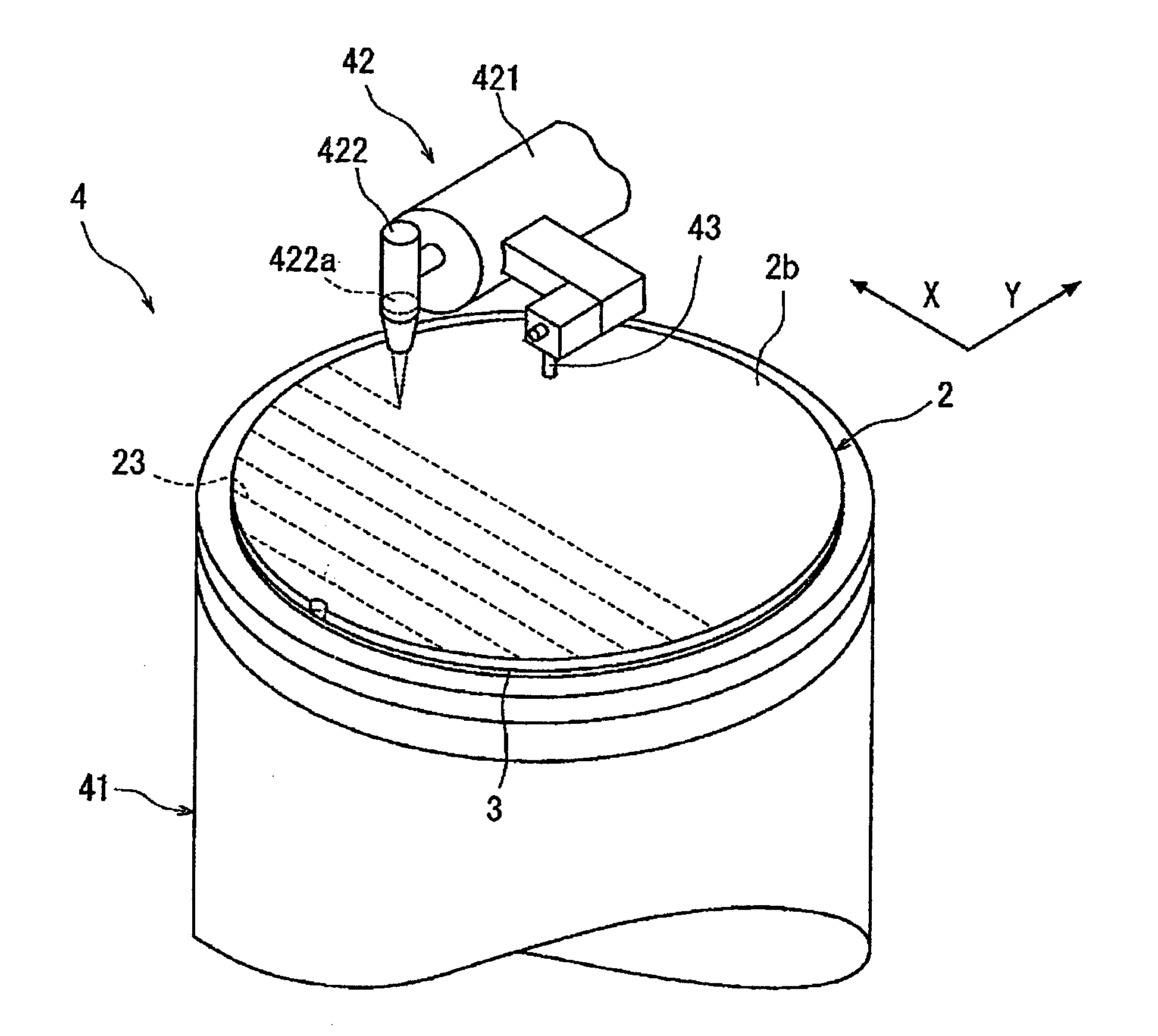
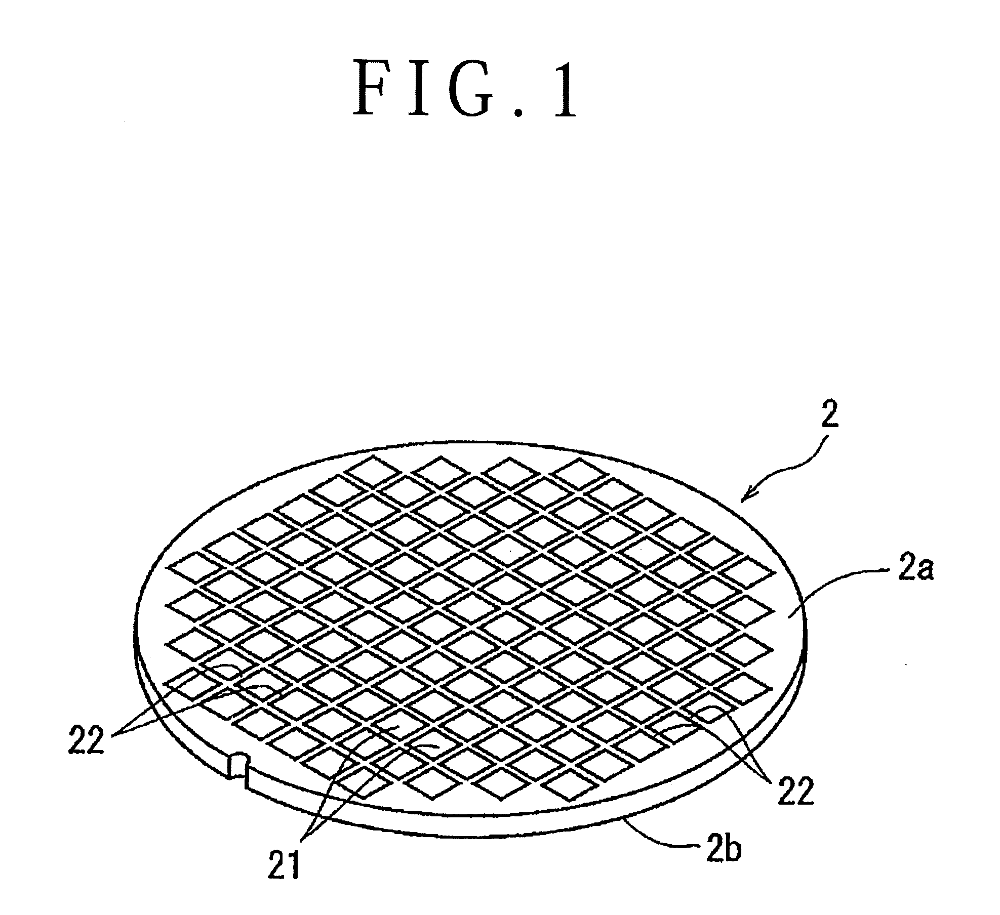
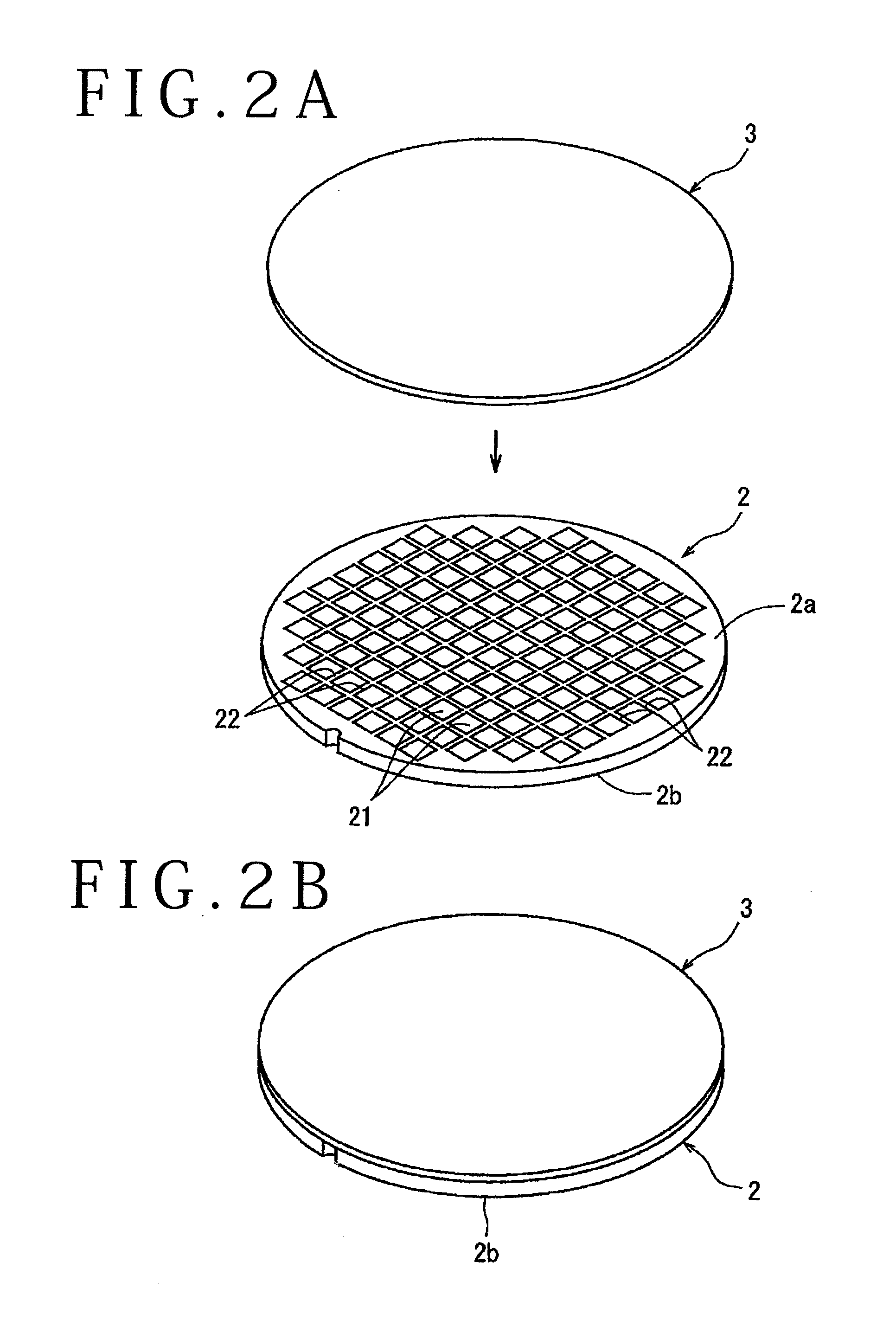
[0021]The wafer processing method according to the present invention will now be described in detail with reference to the attached drawings. FIG. 1 is a perspective view of an optical device wafer 2 as a wafer to be processed by the wafer processing method according to the present invention. The optical device wafer 2 shown in FIG. 1 is composed of a sapphire substrate having a thickness of 300 μm, for example, and a plurality of optical devices 21 such as light emitting diodes and laser diodes formed on the front side 2a of the sapphire substrate so as to be arranged like a matrix. These optical devices 21 are partitioned by a plurality of crossing division lines 22 called streets formed on the front side 2a of the sapphire substrate, i.e., the front side of the optical device wafer 2. While the division lines 22 are clearly formed on the front side 2a of the optical device wafer 2 as shown in FIG. 1, there is also a case that division lines are not clearly formed on a glass plate...


PUM

PropertyMeasurementUnit
Wavelengthaaaaaaaaaa

Abstract

A wafer processing method for dividing a wafer along a plurality of division lines to obtain a plurality of individual chips. The wafer processing method includes a filament forming step of applying a pulsed laser beam having a transmission wavelength to the wafer along each division line in the condition where the focal point of the pulsed laser beam is set inside the wafer in a subject area to be divided, thereby forming a plurality of amorphous filaments inside the wafer along each division line, and an etching step of etching the amorphous filaments formed inside the wafer along each division line by using an etching agent to thereby divide the wafer into the individual chips along the division lines.

Description

BACKGROUND OF THE INVENTION[0001]1. Field of the Invention[0002]The present invention relates to a wafer processing method for dividing a wafer such as a semiconductor wafer and an optical device wafer along a plurality of division lines to obtain a plurality of individual chips.[0003]2. Description of the Related Art[0004]As well known in the art, in a semiconductor device fabrication process, a functional layer composed of an insulating film and a functional film is formed on the front side of a substrate such as a silicon substrate, and a plurality of semiconductor devices such as ICs and LSIs are formed like a matrix from this functional layer, thus obtaining a semiconductor wafer having the plural semiconductor devices. The plural semiconductor devices are partitioned by a plurality of crossing division lines formed on the front side of the semiconductor wafer. The semiconductor wafer is divided along these division lines to obtain the individual semiconductor devices as chips....

Claims


Application Information

Patent Timeline
IPC IPC(8): H01L21/78
CPCH01L21/78B23K26/53B23K26/00B23K26/0648
Inventor MORIKAZU, HIROSHITAKEDA, NOBORU
Owner DISCO CORP
Why Eureka
Try Eureka