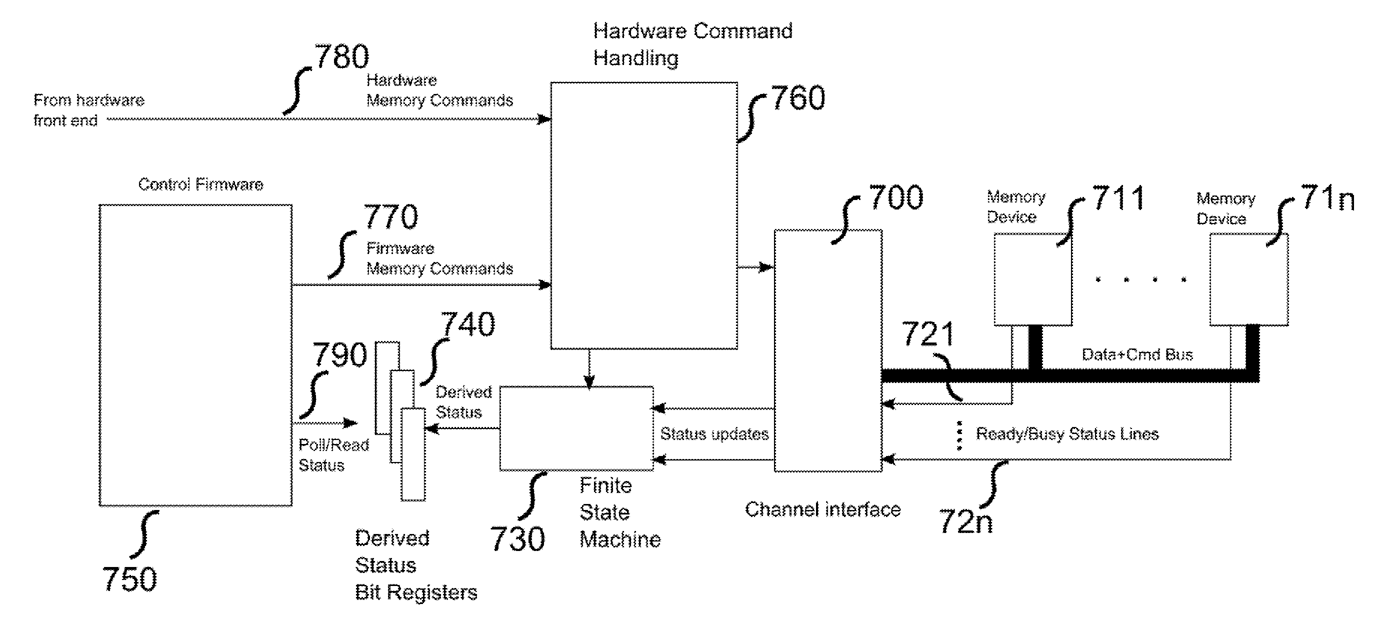
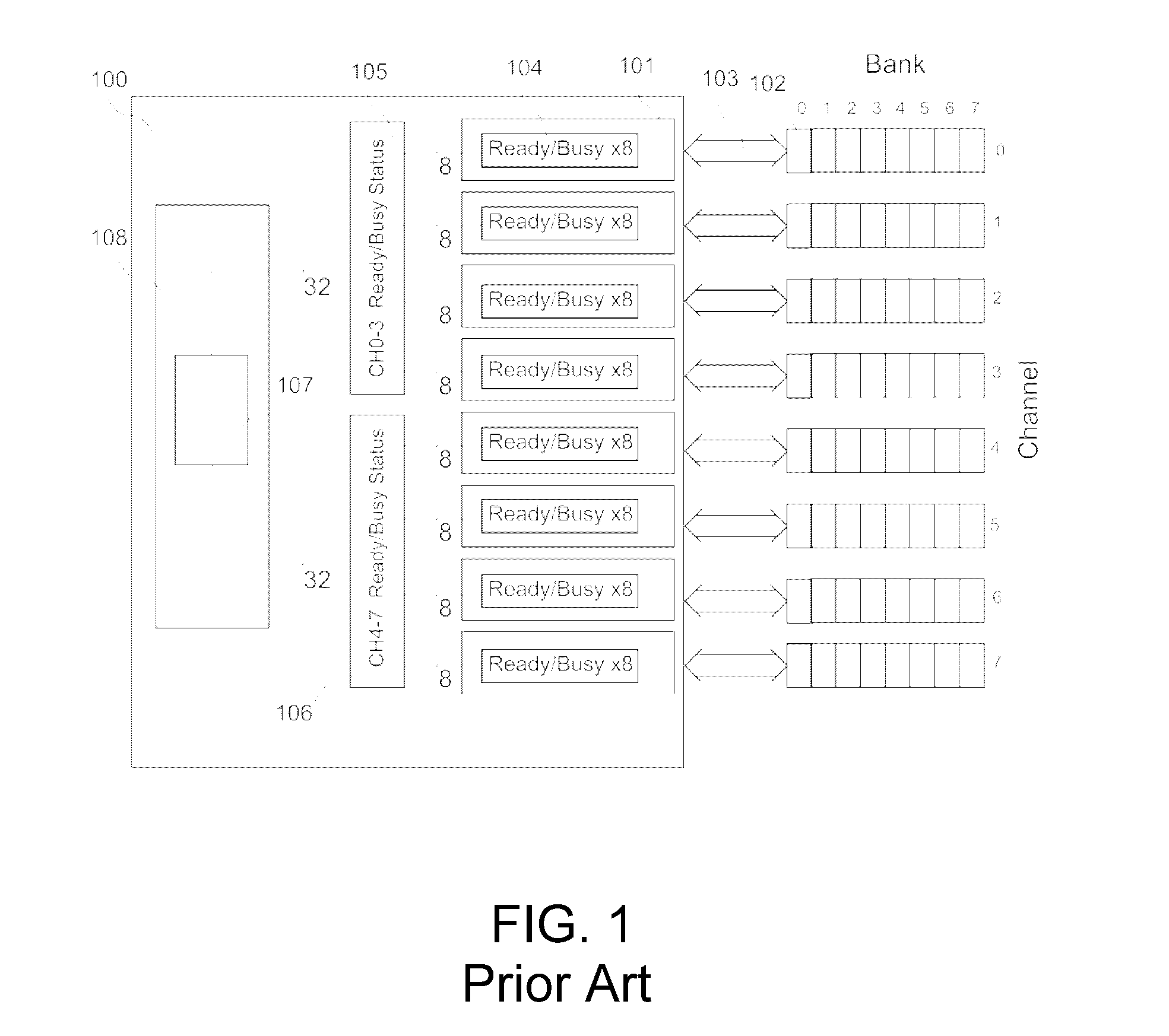
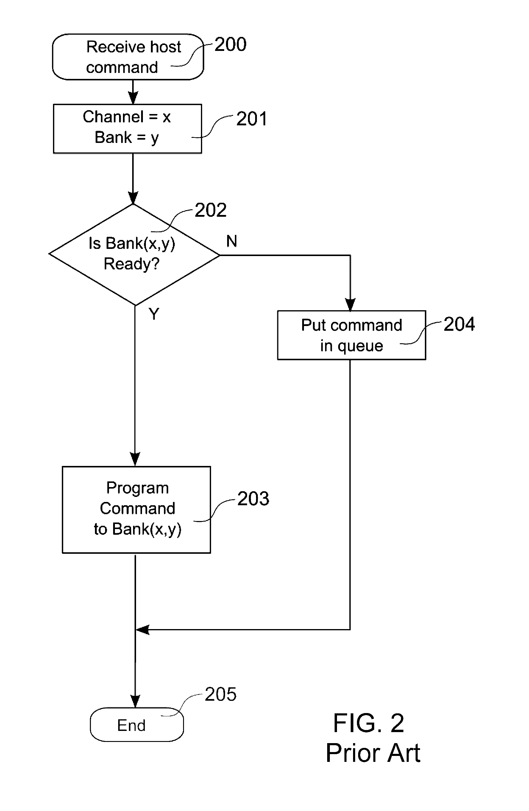
[0024]Certain commands to a non-volatile memory device can only be issued one at a time. For instance, there are commands which, once they are issued and being processed must complete before a new command can be issued to that device. There are also commands which, once they are issued and being processed, can allow only certain other commands to be issued. New commands may be issued to other devices on the same channel, but if another command arrives for a device that is currently processing a command, it may have to wait and be placed in a FIFO (First In, First Out) queue, waiting for the currently processing command to complete before the next command in the queue can be issued.
[0025]The state of the memory device which indicates whether it is currently processing a command is the Ready/Busy# status, which can be either a physical status output pin on the device, or in data returned after issuing a status command. Simply polling the status regularly indicates that a device is ready to accept a new command, but a further check is required to see if a command is queued for that device.
[0026]A preferred aspect of the invention is that an extra check can be avoided if it is realized that a command can only be queued if the status is currently Ready and was previously Busy. The reasoning is that if, on the contrary, the previous status was Ready, then the command would have been processed at that time. Consequently, if the current status is Ready and the previous status was Ready, there can be no command queued and it is not necessary for the extra check to be made.
[0027]Hence, a preferred aspect of the invention is to provide a more efficient mode of polling that takes the current Ready/Busy status, CRB, and the previous Ready/Busy status, PRB, and combines them to form a Now Ready Previously Busy status, NRPB, according to the following logical equation: NRPB Equals CRB AND NOT PRB. A single test of CQR NOT Equals 1 can be sufficient to know that the device is either not ready to accept a new command or that no command is queued waiting to be processed. Applying such a test, if NRPB Equals 1, then the device is ready to accept a new command which may be queued for that device.
[0028]A non-volatile memory controller, according to the current state of the art, provides a plurality of memory bus channels, each of which may be attached to a plurality of individual memory device banks. Referring to FIG. 1, a non-volatile memory controller 100, is shown as attached via eight memory channels 103, which in turn are connected to eight memory banks 102. Each memory channel 103 is shown as connected to a channel controller 101, which contains a state machine 104 that maintains a Ready/Busy status of the eight memory banks 102 attached to that channel 103. The status bits of the various channels 103 may be combined into one of more registers, such as 32-bit registers 105 and 106, for more convenient reading in one operation by a polling loop 107 contained within firmware 108 of the controller 100.
[0029]As shown in the flow chart of FIG. 2, when commands such as those for reading and writing of data are received from a host system to be sent to a memory array 200, they will be translated into commands assigned to a specific memory bank, identified by the channel number (x) and bank number (y) 201 and sent to the appropriate channel controller. If memory bank (x,y) is Ready 202, the command can be programmed directly to Bank (x,y) 203. If Bank (x,y) is busy, the command is placed in a queue 204. The command processing then ends 205.
[0030]To process queued commands, a polling loop is often used, as shown in the flow chart of FIG. 3. The loop starts 300 and initializes the memory channel and memory bank indices Chan and Bank 301. Each memory bank is tested to see if Ready status is set 302 and if not the Chan and Bank indices are incremented 304 then a test is made to see if all the memory banks have been tested 306 and the loop either ends 307 or continues to test the next bank for Ready status 302. If the memory bank was ready at 302, a test is made to see if a command is queued for that bank 303 and if so the command is programmed to that bank 305 and the loop continues by selecting the next bank 304.
[0031]Such a loop is inefficient as it tests all the banks that are ready to see if they have a command queued. In general, there will be fewer banks with queued commands than the number of banks that are ready, so that some tests for the bank being ready are wasted as there is no command queued for that bank.
[0032]FIGS. 4a, 4b, and 5 represent methods in accordance with preferred but nonlimiting aspects of the present invention. These methods may be implemented with a memory controller similar to the one represented in FIG. 1; however, it is foreseeable that implementing portions of the hereinafter described methods with specifically tailored hardware components may be more efficient. Referring to FIG. 4a, the command status 400 enters the command processing state after a command is received 402 and then reverts to idle as the processing finishes 404. The memory bank's Ready/Busy status 410 reflects this as the memory device becomes Busy 412 at the same time as the command processing begins 402 and becomes Ready 414 as the command processing ends 404. The channel controller polls this status of the memory bank at intervals, 450-454, to provide the polled Ready/Busy status 420 which becomes Busy 422 at the next polling event 450 after the command processing begins 402 and becomes Ready again 424 at the next polling event 452 after the command processing ends 404.
[0033]FIG. 4a illustrates the case where a single command arrives and completes with no command arriving in the intervening time. When the command arrives the current polled status 420 is ready and command is sent 402 and starts processing immediately. At the next polling point 450, the status becomes busy 422 and remains busy until the end of the polling interval during which the command completes processing, at which point it becomes ready 424.
[0034]In FIG. 4b, a second command 440 is shown arriving while the first command is processing. Since the polled Ready/Busy state 420 is Busy, the command is queued 440. At the next polling point 451, the Ready/Busy state is still busy and so the command continues to be queued. Only when the first command finishes processing 404 and the memory bank's Ready/Busy status becomes Ready 414 and then becomes polled at the next interval 452 such that the polled Ready/Busy status becomes Ready 424, can the second command be programmed to the bank and start processing 444.
[0035]FIG. 4b shows that a command will be queued if the status is busy, corresponding to a previous command processing. Therefore, the only time a command which is queued needs servicing is when the previous command ends, which results in the status going from busy to ready. It follows that only when the previous status was busy and the current status is ready is there a need to service a queued command.
[0036]In FIGS. 4a and 4b, a status signal which indicates “Now Ready, Previously Busy” (NRPB) 430 becomes true at 432 and becomes false at 434. The polled ready/Busy status also becomes true (ready) at 424 but remains true at 426 and remains so until a succeeding command is processed. Therefore, checking for NRPB being true can avoid having to check during the interval 426 and succeeding intervals, as a prior art check for Ready/Busy being true would involve.
[0037]FIG. 5 shows a flow chart of the processing loop using a ‘Now Ready, Previously Busy’ (NRPB) register which has one bit assigned to each memory bank in the system. Each bit indicates if the bank it represents has changed from busy (0) to ready (1) since the last time the Ready/Busy status of the bank was polled. The loop starts 500 and reads the NRPB register 501. A bit index is set to zero 502, where the bit index is used to represent a memory bank on a channel, then each memory bank is tested to see if Ready status is set by testing if the NRPB register bit referenced by the bit index is set 503 and if not the bit index is incremented 506. A test is then made to see if this is the last bit index and all the banks have been tested 507 and the loop either ends 508 or continues to test the next bit index 503. If the register bit was set at 503 (meaning the corresponding memory bank was ready), a test is made to see if a command is queued for that bank 504 and if so the command is programmed to that bank 505 and the loop continues by selecting the next bank by incrementing the bit index 506.
[0038]The “Now Ready, Previously Busy” (NRPB) 430 status of the memory bank may be determined by the channel controller and will be referred to hereinafter as a derived status of the memory bank. The derived status of each memory bank corresponding to a channel may be maintained in the state machine of the corresponding channel controller. As such, the state machine stores a derived status of each memory bank, which is updated either automatically by hardware, for example, when the physical pin changes state, or on instruction from software on each polling event. The state machine may further change the derived status upon other events such as a new command being sent to the memory device, data being received from the memory device, etc. The derived statuses of each state machine may further be stored in a hardware register or status register. Such an arrangement may be more efficient as it allows software to obtain the derived statuses of all the memory banks from one or more status registers rather than having to communicate with all of the channel controllers individually. Consequently, the derived status of a memory bank is preferably read from a status register during the polling loop. The precise number of bits, status registers, and/or status register width will depend on the number of channels, number of banks on each channel, and the processing capabilities of the memory controller.
[0039]FIG. 6 represents one possible implementation of a process as described above. In FIG. 6, a channel interface 700 of a memory controller provides a hardware bus interface to memory devices (banks) on a channel, memory device 711 to memory device 71n. Each memory device may also be connected by a Ready/Busy status line, 721 to 72n, to the channel interface 700. In a typical memory controller, there may be a number of separate channel interfaces (not shown), each with an identical arrangement and connections to memory devices. The channel interface 700 provides updates of the memory status to a finite state machine 730, which combines current and previous statuses to form a derived status which is passed to derived status bit registers 740. Firmware 750 of the memory controller may issue memory commands 770 to a hardware command handling component 760, which also handles direct memory commands 780 from a hardware front end. The firmware memory commands 770 may include status command requests to memory devices as an alternative arrangement to obtaining the ready/busy status via dedicated status lines 721 to 72n. Regardless of the arrangement adopted, the derived status 740 may be polled or read 790 by the firmware 750.
[0040]While the invention has been described in terms of specific embodiments, it is apparent that other forms could be adopted by one skilled in the art. For example functionally equivalent memory technology may supersede the PCM, RRAM, MRAM, FeRAM and NAND flash memory taught in this disclosure. In addition, the assembly could differ in appearance and construction from the embodiments shown in the Figures, the functions of each component of the device could be performed by components of different construction but capable of a similar (though not necessarily equivalent) function, processing parameters such as time intervals and durations could be modified. Therefore, the scope of the invention is to be limited only by the following claims.