Assembly Structure with Filter Device and Printed Circuit Board and Welding Method for Making the Same

a filter device and printed circuit board technology, applied in the field of assembly structures with filter devices and printed circuit boards, can solve the problems of difficulty and assembling cost of disposing conventional filter devices onto printed circuit boards, and engineers must spend a lot of time finishing welding ways, so as to achieve the effect of reducing manufacturing time and cost of assembly structures, simple process procedures, and effective increase of assembly structure fabrication yield

Inactive Publication Date: 2014-09-11
U D ELECTRONIC CORP +2
View PDF0 Cites 22 Cited by
  • Summary
  • Abstract
  • Description
  • Claims
  • Application Information

AI Technical Summary

Benefits of technology

[0008]The primary objective of the present invention is to provide an assembly structure with filter device and printed circuit board and a welding method for making the same, in which, The welding method is firstly make the metal lines of at least one filter devices be disposed in the metal notches formed on at least one edges of the printed circuit board, and then respectively remove the insulation layers covering the metal lines; therefore, the welding metal lines can be

Problems solved by technology

However, because the size of the conventional filter device is gradually designed and fabricated to be smaller than the size of the traditional filter device, that enhances the difficulty and assembling cost for disposing the conventional filter

Method used


Image

  • Assembly Structure with Filter Device and Printed Circuit Board and Welding Method for Making the Same
  • Assembly Structure with Filter Device and Printed Circuit Board and Welding Method for Making the Same
  • Assembly Structure with Filter Device and Printed Circuit Board and Welding Method for Making the Same

Examples


Embodiment Construction

[0030]To more clearly describe an assembly structure with filter device and printed circuit board and welding method for making the same according to the present invention, embodiments of the present invention will be described in detail with reference to the attached drawings hereinafter.

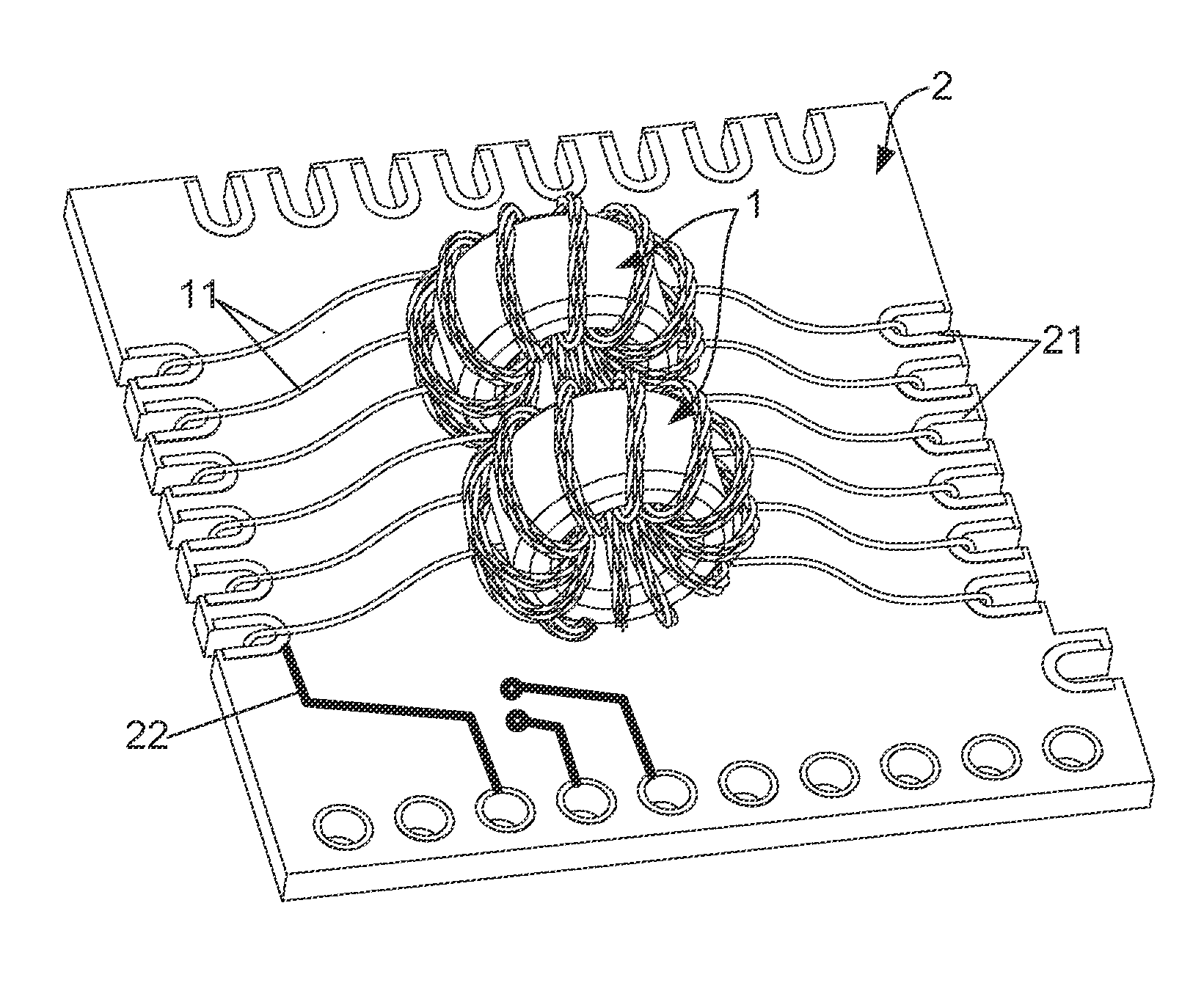
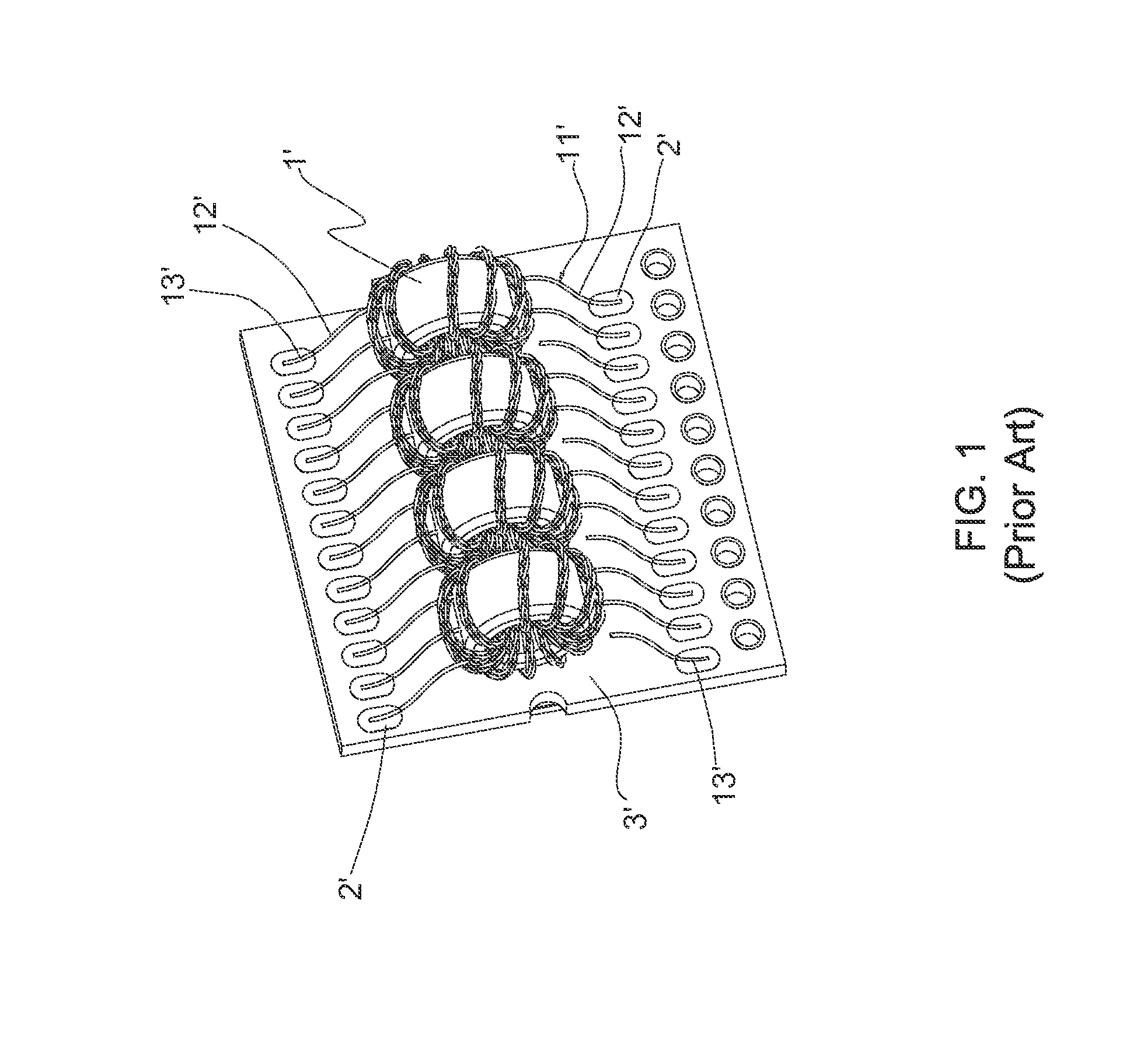
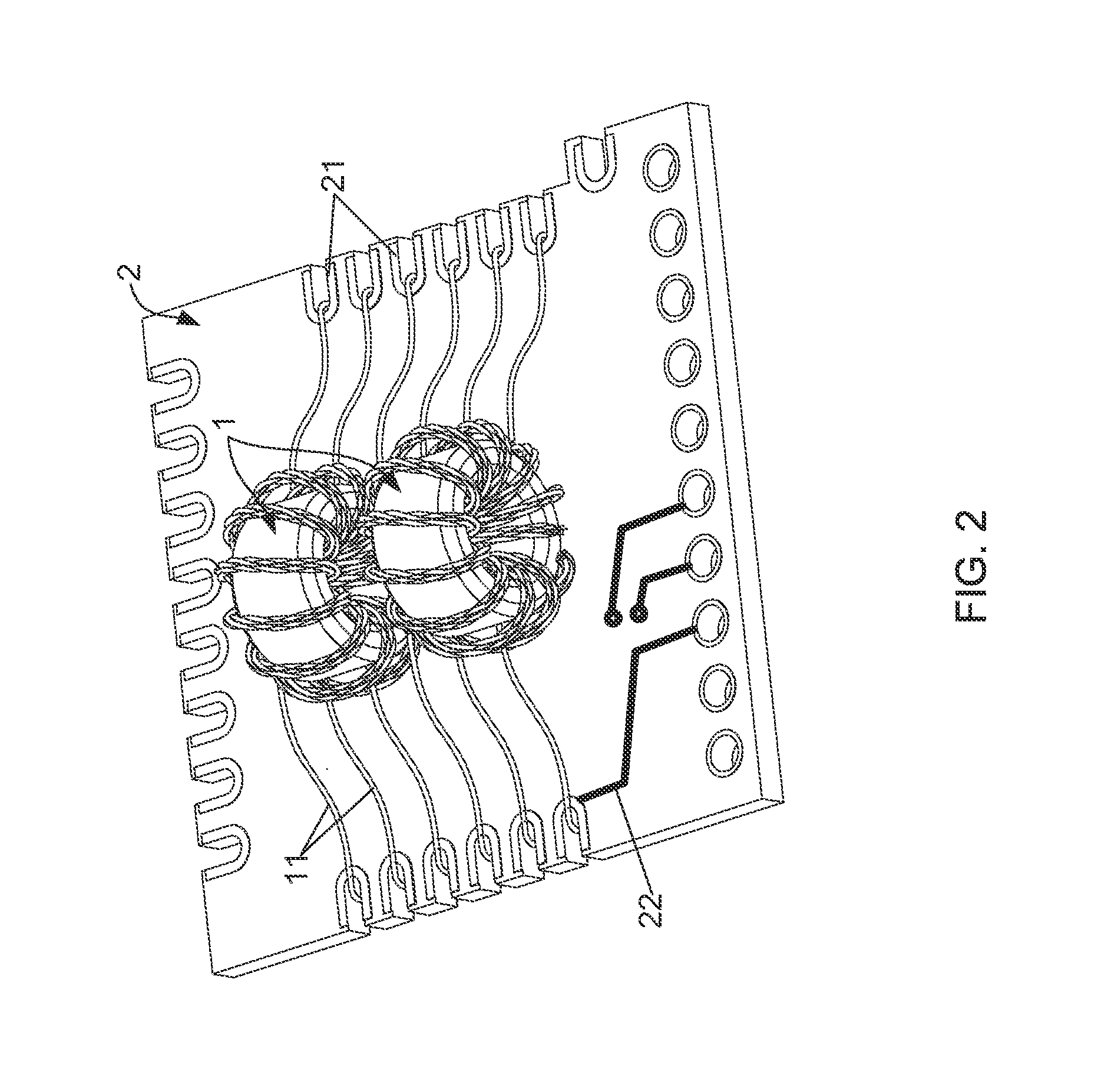
[0031]With reference to FIG. 2, which illustrates a stereo view of an assembly structure with filter devices and printed circuit board. Moreover, please simultaneously refer to FIG. 3, there is shown a cross-sectional view of a metal line. As shown in FIG. 2 and FIG. 3, the assembly structure of with filter devices and printed circuit board proposed by the present invention consists of: a plurality of filter devices 1 and a printed circuit board (PCB) 2, wherein the filter devices 1 are disposed on the PCB 2 and has a plurality of metal lines 11. As FIG. 3 shows, each metal line 11 is consisted by an insulation layer 111 and a copper line 112 covered by the insulation layer 111. In addition, as FIG...


PUM


Abstract

The present invention relates to an assembly structure with filter device and printed circuit board and a welding method for making the same. The welding method is firstly make the metal lines of at least one filter devices be disposed in the metal notches formed on at least one edges of the printed circuit board, and then respectively remove the insulation layers covering the metal lines; therefore, the welding metal lines can be respectively welded with the metal notches after the metal lines and the metal notches are treated with a dip soldering process. Thus, the welding process of the filter device and the printed circuit board can be carried out on the edges of the printed circuit board by simple process procedures; moreover, the fabrication yield of the assembly structure can be effectively increased, and the manufacturing time and cost of the assembly structure can be simultaneously reduced.

Description

BACKGROUND OF THE INVENTION[0001]1. Field of the Invention[0002]The present invention relates to the technology field of electrical connectors, and more particularly to an assembly structure with filter device and printed circuit board and a welding method for making the same.[0003]2. Description of the Prior Art[0004]Nowadays, electrical connectors are commonly provided with filter circuits (or units) for blocking or preventing the influences caused by external noise signal. However, because the size of the conventional filter device is gradually designed and fabricated to be smaller than the size of the traditional filter device, that enhances the difficulty and assembling cost for disposing the conventional filter devices onto the printed circuit boards.[0005]In the conventional technologies, the filters 1′ shown in FIG. 1 are welded to the welding pads 2′ of the PCB 3′ by handwork or using specific welding machine; moreover, before welding the filters 1′ onto the PCB 3′, it need...

Claims


Application Information

Patent Timeline
IPC IPC(8): H05K13/04H05K7/14
CPCH05K7/14H05K13/04H05K1/0233H05K3/3421H05K2201/09181H05K2201/1003H05K2201/10651H05K2203/044H05K2203/107H01F17/062H01F27/2828H01F27/292Y02P70/50
Inventor CHANG, CHIH-KAIGUO, TAO
Owner U D ELECTRONIC CORP
Why Eureka
Try Eureka