Non-replacement gate nanomesh field effect transistor with pad regions

a technology of pad region, which is applied in the field of wirefirst, gatefirst nanomesh field effect transistor, can solve the problems of increasing the processing time and manufacturing cost of increasing the amount of current per unit device area, and complex processing steps used to form nanowire field effect transistors

Active Publication Date: 2014-09-18
GLOBALFOUNDRIES US INC
View PDF0 Cites 36 Cited by
  • Summary
  • Abstract
  • Description
  • Claims
  • Application Information

AI Technical Summary

Benefits of technology

[0003]A gate-first processing scheme for forming a nanomesh field effect transistor is provided. An alternating stack of two different semiconductor materials is patterned to include two pad regions connected by nanowire regions. A semiconductor material is laterally etched selective to another semiconductor material to form a nanomesh including suspended semiconductor nanowi...

Problems solved by technology

While nanowire field effect transistors offer the potential for scaling semiconductor devices in future generations, one of the challenges for the nanowire field effect transistors is the amount of current per unit device area.
Another of the challenges for the nanowire field effect transistors is the comp...

Method used


Image

  • Non-replacement gate nanomesh field effect transistor with pad regions
  • Non-replacement gate nanomesh field effect transistor with pad regions
  • Non-replacement gate nanomesh field effect transistor with pad regions

Examples


Embodiment Construction

[0042]As stated above, the present disclosure relates to a wire-first, gate-first nanomesh field effect transistor with epitaxially thickened source and drain regions, and a method of manufacturing the same. Aspects of the present disclosure are now described in detail with accompanying figures. It is noted that like reference numerals refer to like elements across different embodiments. The drawings are not necessarily drawn to scale.

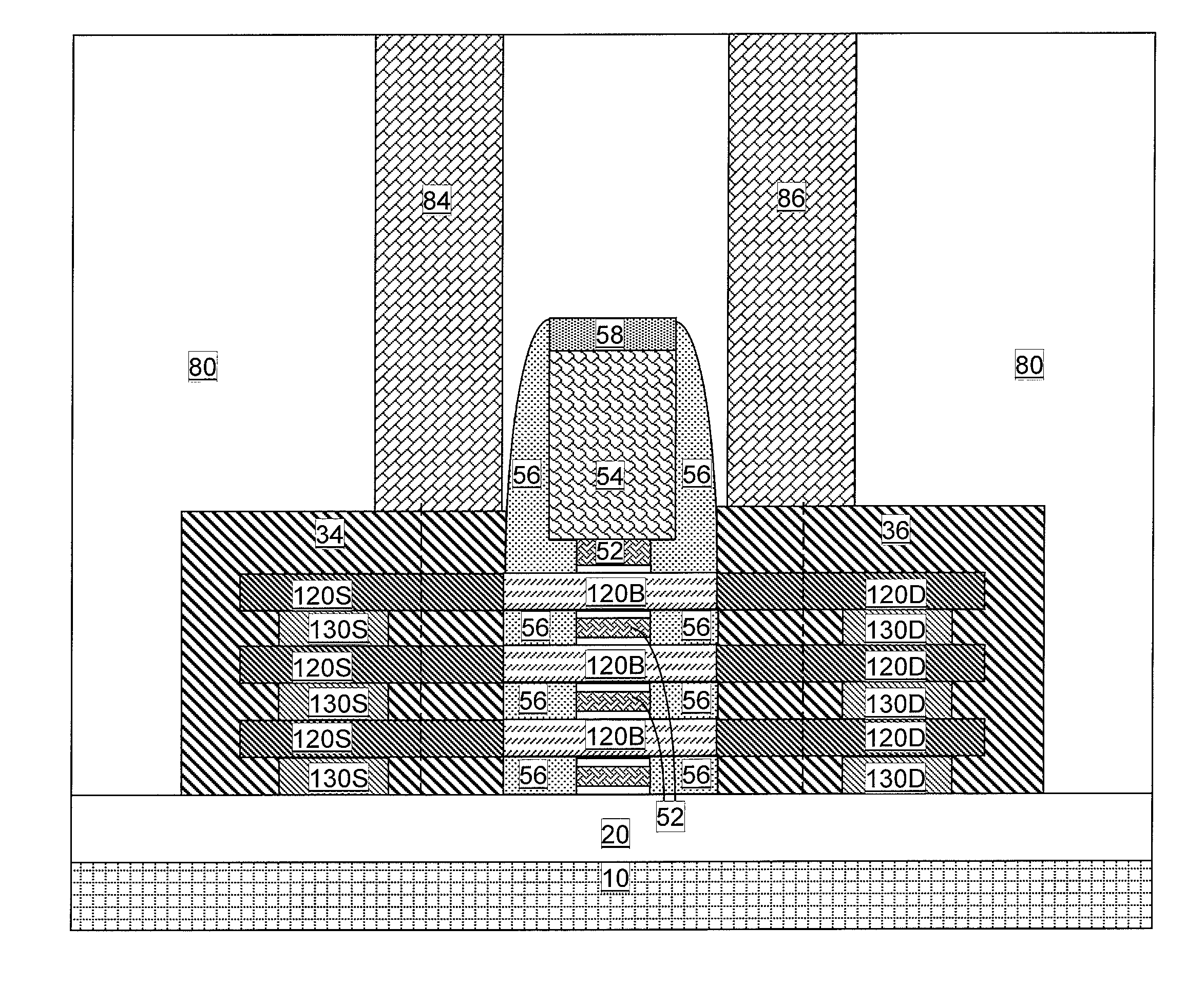
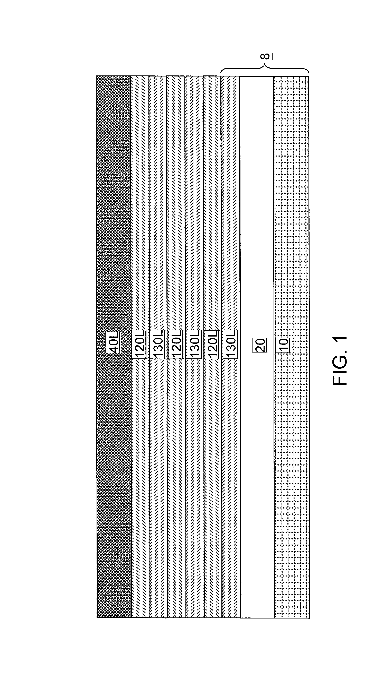
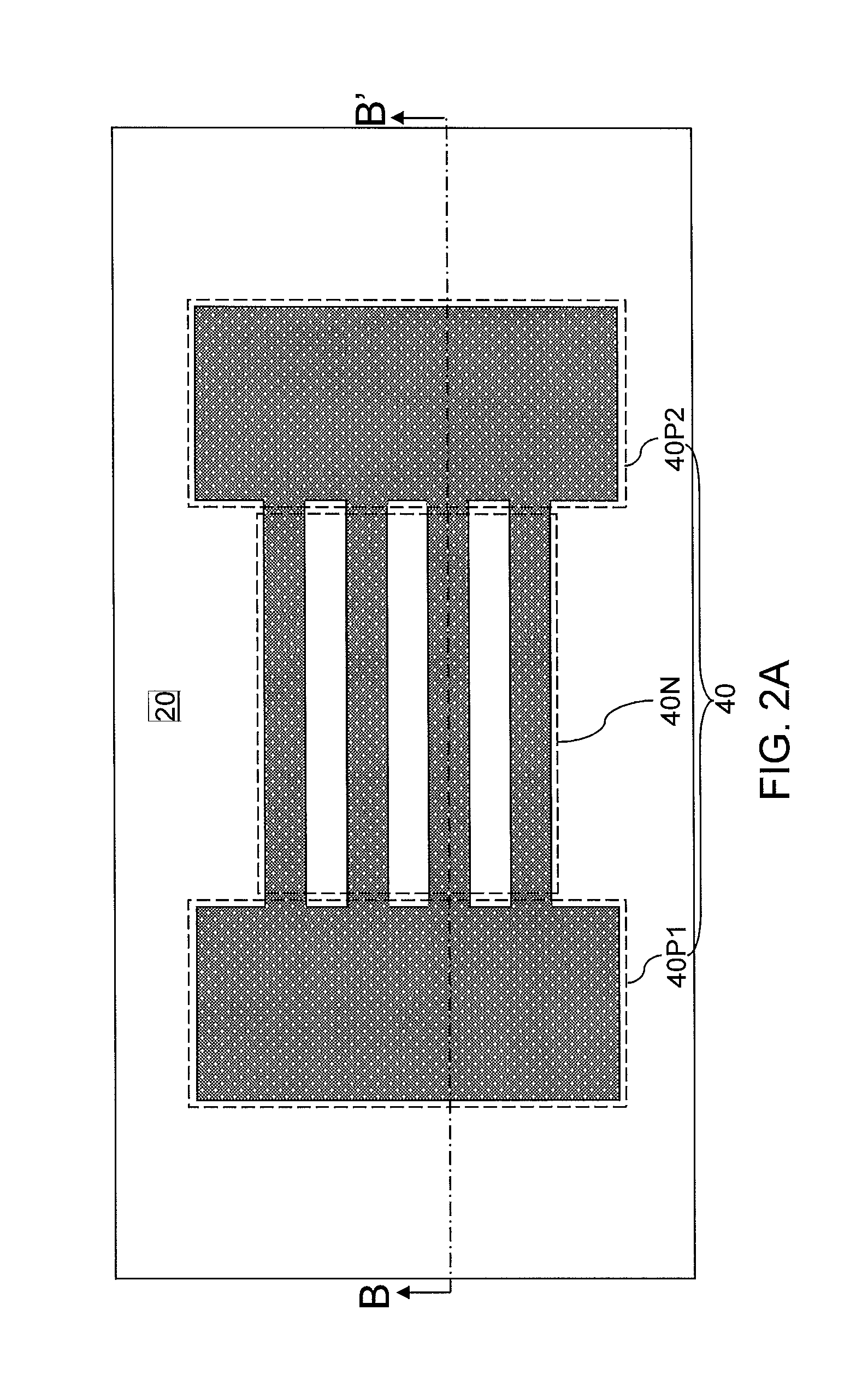
[0043]Referring to FIG. 1, an exemplary semiconductor structure according to an embodiment of the present disclosure can be formed by providing a semiconductor-on-insulator (SOI) substrate 8 including a handle substrate 10, an insulator layer 20, and a single crystalline semiconductor material layer on top of the insulator layer. The handle substrate 10 can include a semiconductor material, an insulator material, and / or a conductive material. The insulator layer 20 can include, for example, silicon oxide, silicon nitride, aluminum oxide, or any other d...


PUM


Abstract

A gate-first processing scheme for forming a nanomesh field effect transistor is provided. An alternating stack of two different semiconductor materials is patterned to include two pad regions and nanowire regions. A semiconductor material is laterally etched selective to another semiconductor material to form a nanomesh including suspended semiconductor nanowires. A stack of a gate dielectric, a gate electrode, and a gate cap dielectric is formed over the nanomesh. A dielectric spacer is formed around the gate electrode. An isotropic etch is employed to remove dielectric materials that are formed in lateral recesses of the patterned alternating stack. A selective epitaxy process can be employed to form a source region and a drain region.

Description

BACKGROUND[0001]The present disclosure relates to a semiconductor structure, and particularly to a wire-first, gate-first nanomesh field effect transistor with epitaxially thickened source and drain regions, and a method of manufacturing the same.[0002]While nanowire field effect transistors offer the potential for scaling semiconductor devices in future generations, one of the challenges for the nanowire field effect transistors is the amount of current per unit device area. Another of the challenges for the nanowire field effect transistors is the complexity of processing steps employed to form the nanowire field effect transistors. Particularly, processing steps to form a replacement gate structure over nanowires introduce many additional processing steps, thereby increasing the processing time and the manufacturing cost for nanowire field effect transistors.BRIEF SUMMARY[0003]A gate-first processing scheme for forming a nanomesh field effect transistor is provided. An alternatin...

Claims


Application Information

Patent Timeline
IPC IPC(8): H01L29/775H01L29/66
CPCH01L29/66439H01L29/775B82Y10/00H01L29/0673H01L29/42392H01L29/66469H01L29/78696
Inventor CHANG, JOSEPHINE B.CHANG, PAULLAUER, ISAACSLEIGHT, JEFFREY W.
Owner GLOBALFOUNDRIES US INC
Why Eureka
Try Eureka