Heat slug having thermoelectric elements and semiconductor package including the same

a technology of heat dissipation elements and heat slugs, which is applied in the direction of semiconductor devices, machines using electric/magnetic effects, refrigerating machines, etc., can solve the problems of significant limitation of temperature sensors, temperature sensors cannot be positioned at desirable sites in semiconductor packages, and the allowable space for temperature sensors is gradually reduced, so as to improve the efficiency of heat dissipation of soc and the number of functional units

Inactive Publication Date: 2014-09-18
SAMSUNG ELECTRONICS CO LTD
View PDF7 Cites 17 Cited by
  • Summary
  • Abstract
  • Description
  • Claims
  • Application Information

AI Technical Summary

Benefits of technology

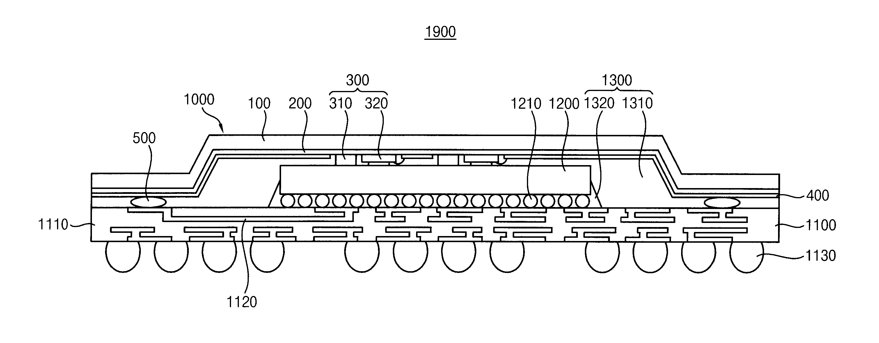
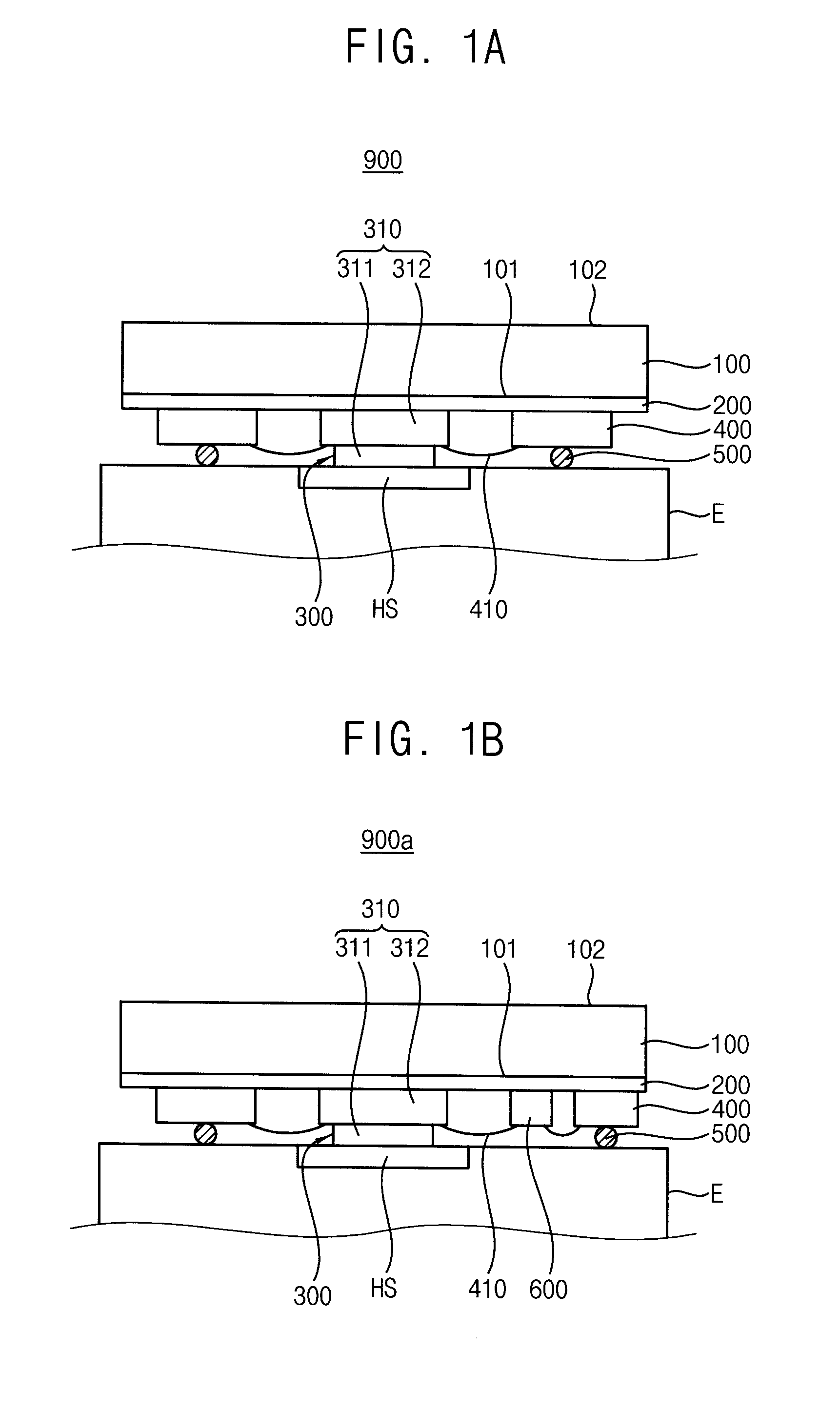
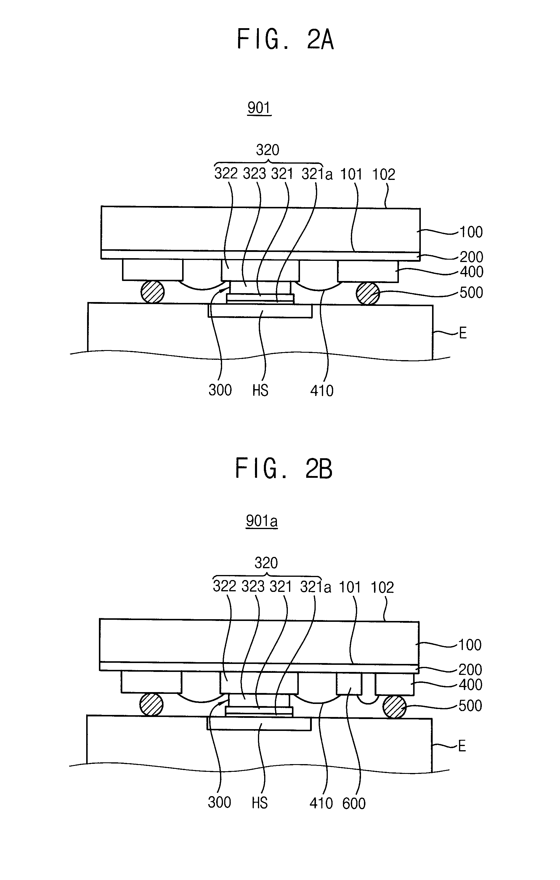
[0032]In an embodiment having the SoC structure in which a plurality of functional unit chips may be arranged in a single die and the amount of heat from each unit chip may be different from one another, the temperature detector and the heat transfer unit may be sufficiently provided at each unit chip without the space margin limitation, since the temperature detector and the heat transfer unit may be provided on the heat slug rather than on the unit chip of the SoC. Thereby, the efficiency of the heat dissipation of the SoC is improved. Thus, although the semiconductor package may be downsized and the number of the functional unit chips may increase in the semiconductor chip, the heat may be sufficiently dissipated from each of the unit chips through the active cooling process or the passive cooling process of the heat slug.

Problems solved by technology

However, due to semiconductor packages being manufactured to have smaller sizes and being manufactured to have high package density, the allowable space for the temperature sensors is gradually reduced.
Thus, problems have occurred in which the temperature sensors cannot be positioned at desirable sites in the semiconductor package.
Particularly, in a case in which a system on chip (SoC) having a memory interface and a logic interface such as a central process unit (CPU) arranged on a single chip, a number of the temperature sensors and the sites for the temperature sensors are significantly limited due to the reduced inner space of the SoC.
As a result, the temperature of the chip is difficult to be accurately detected by the temperature sensors.
However, the temperature sensors are actually arranged on peripheral areas of the logic interface or on the memory interface due to the space limitations of the SoC.
As a result, the surface temperature of the logic interface is not accurately detected by the temperature sensors.
In addition, the space limitation of the SoC restricts the number of the temperature sensors in the SoC.
In contrast, when the temperature of the heat source is increased to be higher than the reference temperature due to an instantaneous excessive operation, the heat slug may forcibly transfer the heat outwards from the excessively operated heat source in the active mode by using the heat transfer unit, such as, for example, the peltier device.

Method used


Image

  • Heat slug having thermoelectric elements and semiconductor package including the same
  • Heat slug having thermoelectric elements and semiconductor package including the same
  • Heat slug having thermoelectric elements and semiconductor package including the same

Examples


Embodiment Construction

[0044]Various example embodiments will be described more fully hereinafter with reference to the accompanying drawings, in which some example embodiments are shown. The present inventive concepts may, however, be embodied in many different forms and should not be construed as limited to the example embodiments set forth herein.

[0045]It will be understood that when an element or layer is referred to as being “on,”“connected to” or “coupled to” another element or layer, it can be directly on, connected or coupled to the other element or layer or intervening elements or layers may be present. In contrast, when an element is referred to as being “directly on,”“directly connected to” or “directly coupled to” another element or layer, there are no intervening elements or layers present. Like numerals refer to like elements throughout. As used herein, the term “and / or” includes any and all combinations of one or more of the associated listed items.

[0046]It will be understood that, although...


PUM


Abstract

In a heat slug and a semiconductor package including the same, the heat slug includes a thermal conductive body having an active face and a dissipating face opposite to the active face, a dielectric layer covering the active face of the body, at least one thermoelectric element arranged on the dielectric layer and a conductive pattern arranged on the dielectric layer and electrically connected to the thermoelectric element. The electrical characteristics of the thermoelectric element are interacted with heat generated from a heat source.

Description

CROSS-REFERENCE TO RELATED APPLICATIONS[0001]This U.S. non-provisional application claims priority under 35 U.S.C. §119 to Korean Patent Application No. 10-2013-0027884 filed on Mar. 15, 2013 in the Korean Intellectual Property Office, the contents of which are herein incorporated by reference in their entirety.BACKGROUND[0002]1. Field[0003]Example embodiments of the present inventive concepts relate to a heat slug and a semiconductor package including the same. More particularly, the example embodiments of the present inventive concepts relate to a heat slug having thermoelectric elements and a semiconductor package including the same.[0004]2. Description of the Related Art[0005]As recent electronic devices have been highly integrated with high performance, semiconductor packages are also manufactured to have small size and high density. Higher performance of the high density semiconductor packages at higher speeds generates a larger amount of heat in the semiconductor package. Thu...

Claims


Application Information

Patent Timeline
Patent Type & Authority Applications(United States)
IPC IPC(8): F25B21/02H01L23/38H01L23/34
CPCF25B21/02H01L23/38H01L23/345H01L23/34F25B2321/0212H01L23/36H01L23/49816H01L2224/48091H01L2924/00014
Inventor KIM, JI-CHULHWANG, HEE-JUNGSHIN, SEONG-HO
Owner SAMSUNG ELECTRONICS CO LTD
Why Eureka
Try Eureka