Printed circuit board package structure and manufacturing method thereof

a printed circuit board and package technology, applied in the direction of printed circuit stress/warp reduction, inductance, electric connection formation of printed elements, etc., can solve the problems of reducing the structure strength of the four-layer circuit board, wasting both the material and the process time, and degrading or damaging the electrical characteristics of the magnetic elements, so as to save time and material costs, and enhance the support strength of the printed circuit board package structure. , the effect of reducing the stress affecting the indu

Active Publication Date: 2014-09-18
TRIPOD TECHNOLOGY CORPORATION
View PDF3 Cites 34 Cited by
  • Summary
  • Abstract
  • Description
  • Claims
  • Application Information

AI Technical Summary

Benefits of technology

[0019]In the aforementioned embodiments of the present invention, the printed circuit board package structure is a three-layer package structure. The second metal layer on the second surface of the substrate can be formed as a plurality of second metal portions by patterning, and through the conductive films of the conductive channels, each of the conductive portions electrically connect to a corresponding second metal portion. Compared with a conventional four-layer package structure, the second surface of the substrate does not need to etch all the second metal layer, furthermore, the second surface does not need to laminate an additional conductive layer. The patterned second metal layer (i.e., the second metal portions) is used to electrically connect to the conductive channels. Since the second metal layer is included by the substrate (Copper Clad Laminate) itself, the printed circuit board package structure of the present invention can save the time cost and the material cost of the manufacture processes that were needed at conventional processes of etching all the second metal layer and of laminating the additional conductive layer. Moreover, since the magnetic elements are very sensitive to the stress, the electrical characteristics of the magnetic elements may be degraded or damaged due to the stress causing by the manufacture processes and by the package structure itself. The three-layer package structure allow the thickness of the second metal layer being greater than the thickness of a conventional conductive layer laminated on the second surface, thus enhancing the support strength of the printed circuit board package structure, and reducing the stress which impacts the inductance value.
[0020]The printed circuit board package structure can release the pressure and remove the heat through the gas channels at the outer wall or the inner wall of the ring-shaped concave portion, and through the pressure relief through holes at the adhesive layer and the second protection layer on the adhesive layer, thereby saving the cost by omitting the adhesive material within the ring-shaped concave portion, and reducing the stress causing by the manufacture processes and by the package structure itself to improve the inductance value. Moreover, the printed circuit board package structure can avoid the gas in the ring-shaped concave portion during the IR reflow to expand due to the high temperature, such that the adhesive layer which covers the substrate and the second protection layer on the adhesive layer are not damaged.

Problems solved by technology

Because the magnetic elements are very sensitive to the stress, the electrical characteristics of the magnetic elements may be degraded or damaged due to the environmental stress; both the conventional manufacturing processes and package structures would lead to the stress which impacts the inductance value.
However, before laminating the copper foil on the back side of the substrate, all the cooper on the back side of the CCL is needed to be removed by etching, resulting in the waste of both the material and the cost of the process time, and the thickness of the copper foil is smaller than the copper on the back side of the substrate, thereby reducing the structure strength of the four-layer circuit board and leading to the stress which impacts the inductance value.
In addition, later when the circuit board is under the process of Surface Mount Technology (SMT), in the IR Reflow, the gas at the containing groove easily expands due to the high temperature, thereby leading to the adhesive layer and the epoxy resin covered on the substrate be damaged; unless the adhesive with high quality is used, but if designers do so, the usage of the high quality adhesive will result in the increasing cost.
Moreover, since the magnetic elements are very sensitive to the stress, the electrical characteristics of the magnetic elements may be degraded or damaged due to the stress causing by the manufacture processes and by the package structure itself.

Method used


Image

  • Printed circuit board package structure and manufacturing method thereof
  • Printed circuit board package structure and manufacturing method thereof
  • Printed circuit board package structure and manufacturing method thereof

Examples


Embodiment Construction

[0039]Reference will now be made in detail to the present embodiments of the invention, examples of which are illustrated in the accompanying drawings. Wherever possible, the same reference numbers are used in the drawings and the description to refer to the same or like parts.

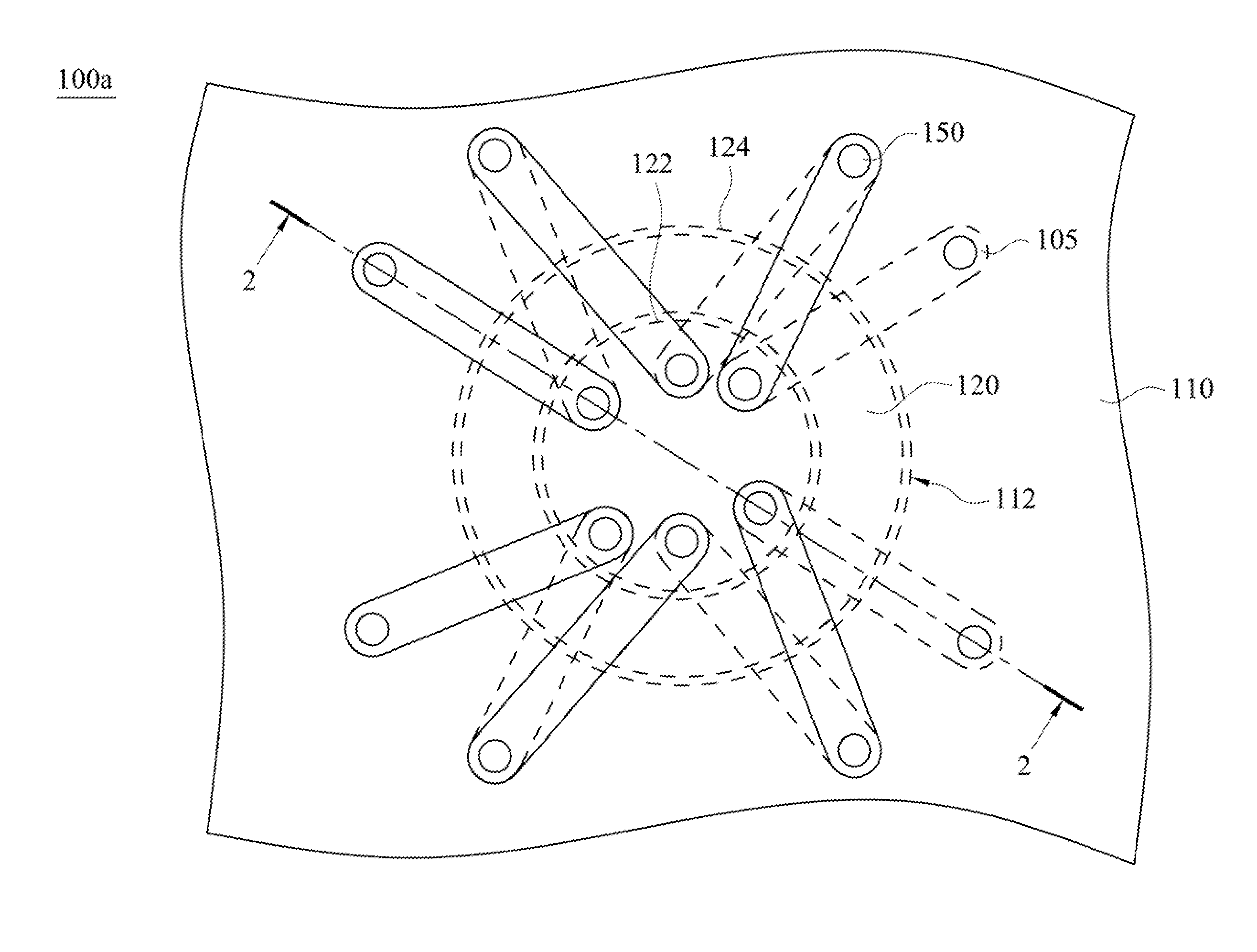
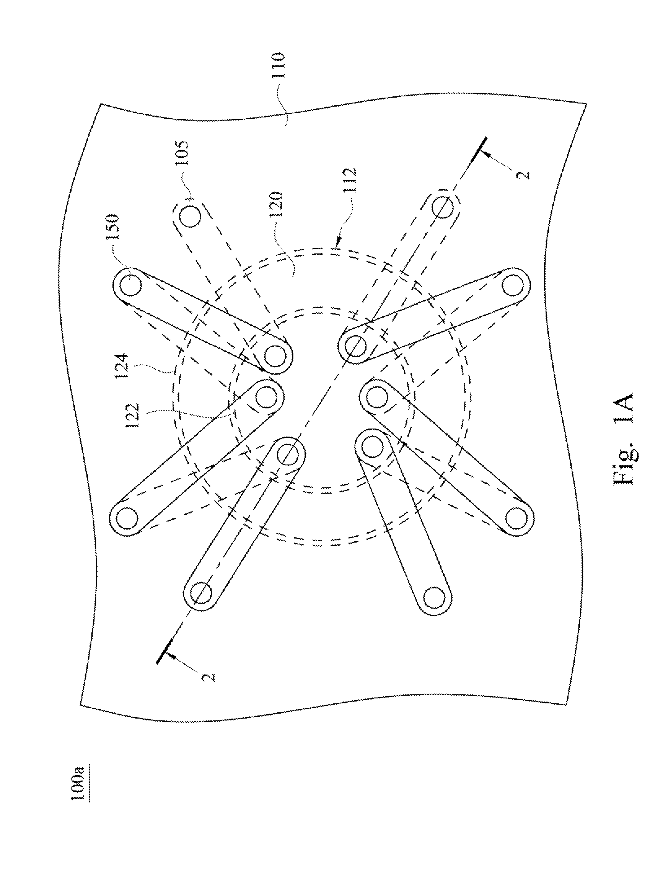
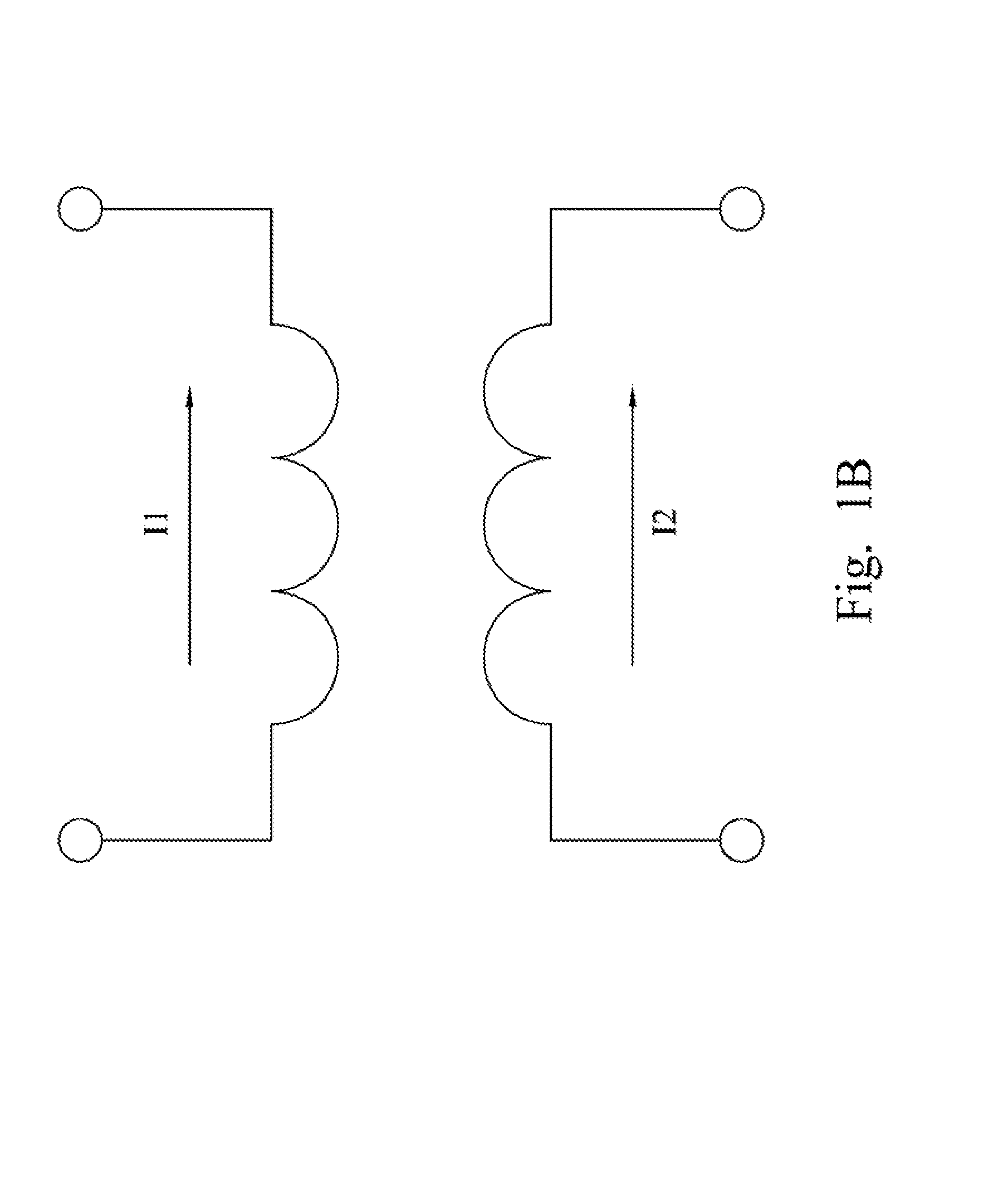
[0040]FIG. 1A is a diagram illustrating a top view of a printed circuit board package structure 100a according to an embodiment of the present invention. FIG. 1B is a schematic view of an equivalent circuit of FIG. 1A. As shown in FIG. 1A and FIG. 1B, the printed circuit board package structure 100a includes a plurality of conductive channels 150 and a plurality of circuits 105. The arrangement of the circuits 105 can be designed according to the requirements of the designer. Among the circuits 105 in FIG. 1A, the ones shown in solid lines are referred to as top layer circuits, and the ones shown in dotted lines are referred to as the bottom layer circuits, vice versa. In this embodiment, the printed circuit b...


PUM

PropertyMeasurementUnit
temperatureaaaaaaaaaa
diametersaaaaaaaaaa
radiusaaaaaaaaaa

Abstract

A printed circuit board package structure includes a substrate having a first surface and a second surface, a ring-shaped magnetic element, an adhesive layer, conductive portions and conductive channels. The first and second surfaces respectively have first and second metal portions. A ring-shaped concave portion is formed on a position not covered by the first metal portions of the first surface. The ring-shaped magnetic element is placed in the ring-shaped concave portion. The adhesive layer covers the first metal portions and the ring-shaped magnetic element. The conductive portions are formed on the adhesive layer. The conductive channels penetrate the conductive portions, the adhesive layer, and the substrate, and are respectively located in an inner wall and outside an outer wall of the ring-shaped concave portion. Each of the conductive channels includes a conductive film electrically connects to the aligned conductive portion and second metal portion.

Description

RELATED APPLICATIONS[0001]This application claims priority to Taiwan Application Serial Number 102108881, filed Mar. 13, 2013, which is herein incorporated by reference.BACKGROUND[0002]1. Field of Invention[0003]The present invention relates to a printed circuit board package structure and a manufacturing method thereof.[0004]2. Description of Related Art[0005]Generally, during the manufacturing processes of the circuit boards, specific elements are required to be located into a predetermined containing groove of the circuit board, such as the cooling cooper block and the cooling iron core. The iron core can be applied into the structure of the transformer or the structure of the power choke since the iron core is with magnetism. Because the magnetic elements are very sensitive to the stress, the electrical characteristics of the magnetic elements may be degraded or damaged due to the environmental stress; both the conventional manufacturing processes and package structures would le...

Claims


Application Information

Patent Timeline
Patent Type & Authority Applications(United States)
IPC IPC(8): H05K1/02H05K3/42H01F27/28
CPCH05K1/0271H05K3/429H01F27/2804H01F17/0033H01F17/062H05K1/165H05K3/4602H05K3/4652H05K2201/029H05K2201/086H05K2201/09636H05K2203/1178Y10T29/49165
Inventor HUANG, BO-SHIUNGYANG, WEI-HSIUNGSHIH, HAN-CHINGLIN, CHENG-FENG
Owner TRIPOD TECHNOLOGY CORPORATION
Why Eureka
Try Eureka