Method and Apparatus for Extracting Systematic Defects

Active Publication Date: 2014-09-18
TAIWAN SEMICON MFG CO LTD
View PDF3 Cites 44 Cited by
  • Summary
  • Abstract
  • Description
  • Claims
  • Application Information

AI Technical Summary

Problems solved by technology

However, these advances have increased the complexity of processing and manufacturing ICs.
However, these inspections may identify a huge number of potential defects.
However, the SEM tools can only review a very small portion of the wafer at a time.
In other words, the SEM review is a time-consuming process.
Generally, it is simply no

Method used


Image

  • Method and Apparatus for Extracting Systematic Defects
  • Method and Apparatus for Extracting Systematic Defects
  • Method and Apparatus for Extracting Systematic Defects

Examples


Embodiment Construction

[0012]It is to be understood that the following disclosure provides many different embodiments, or examples, for implementing different features of the invention. Specific examples of components and arrangements are described below to simplify the present disclosure. These are, of course, merely examples and are not intended to be limiting. In addition, the present disclosure may repeat reference numerals and / or letters in the various examples. This repetition is for the purpose of simplicity and clarity and does not in itself dictate a relationship between the various embodiments and / or configurations discussed.

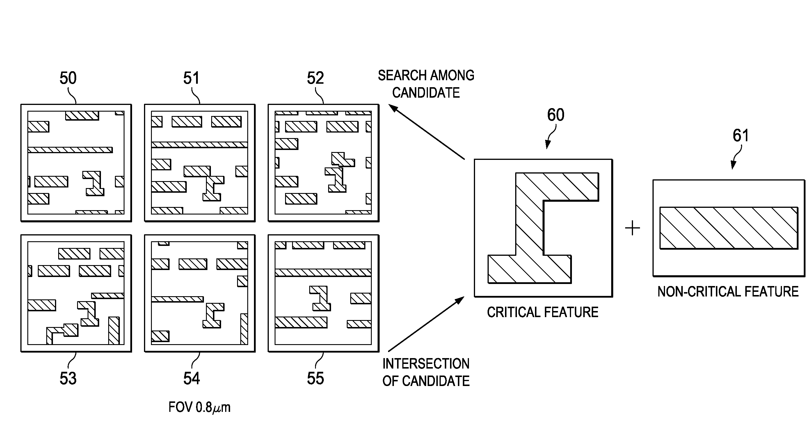
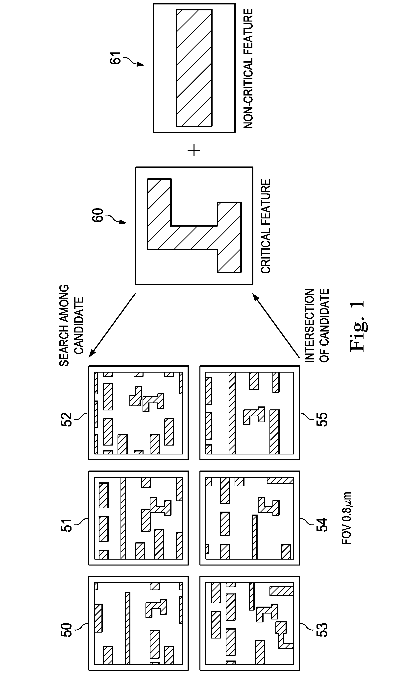
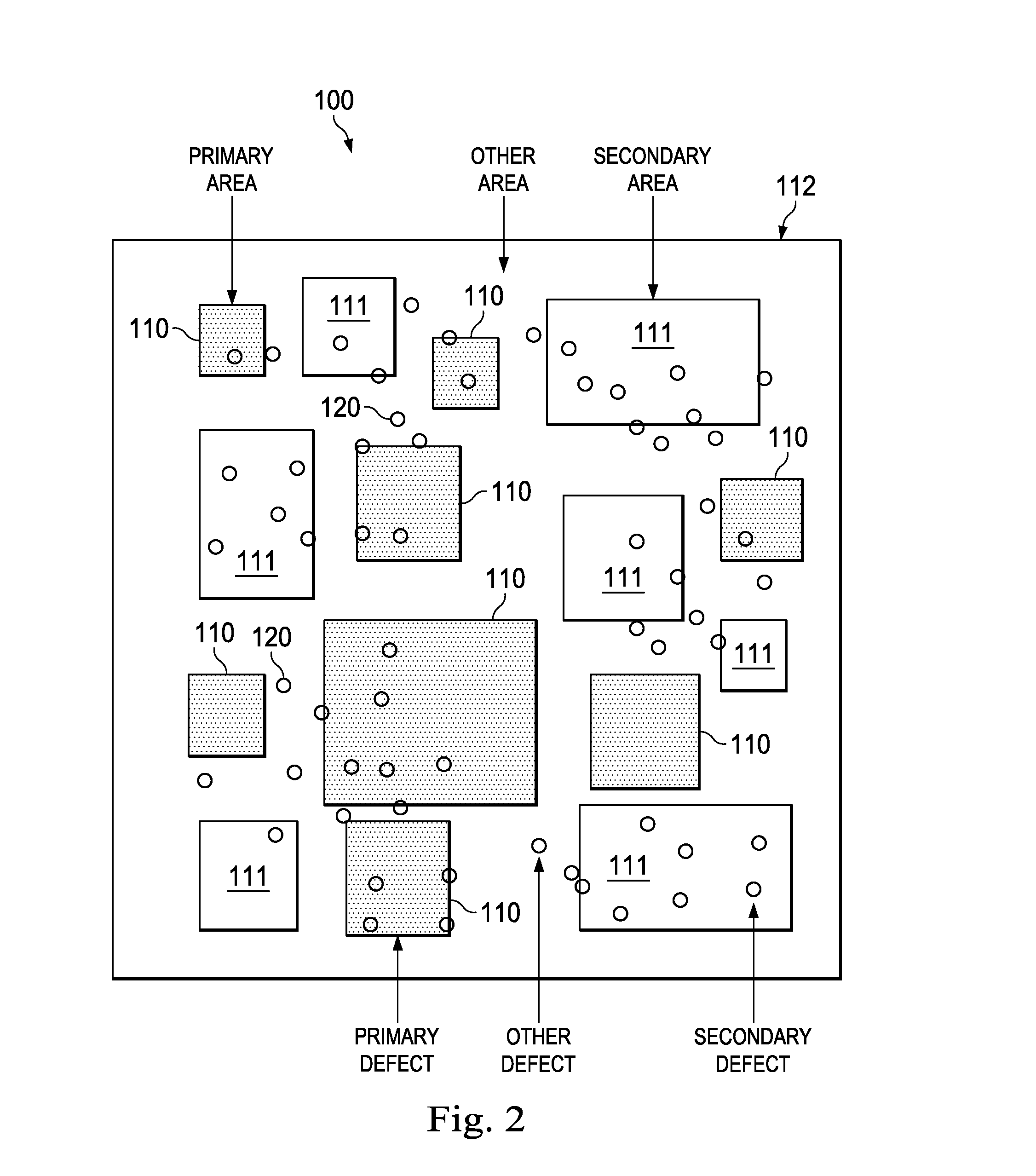
[0013]As a part of the IC fabrication process, wafers may undergo inspection to identify potential defects. For a standard wafer inspection process, defects that are identified may include systematic defects, systematic random defects, and random or nuisance defects. Systematic defects and systematic random defects are often collectively referred to as a “hot spot.” Such hot...


PUM


Abstract

The present disclosure provides a method of systematic defect extraction. Primary and secondary areas are defined in a wafer layout. A plurality of defects is identified by a first wafer inspection for an outside-process-window wafer. Defects located in the secondary area are removed. Defects associated with non-critical semiconductor features are also removed via a grouping process. Sensitive regions are defined around defects associated with critical semiconductor features. A second inspection is then performed on the sensitive regions for an inside-process-window wafer, thereby identifying a plurality of potentially systematic defects. Thereafter, a Scanning Electron Microscopy (SEM) process is performed to determine whether the defects in the sensitive regions of the inside-process-window wafer are true systematic defects.

Description

PRIORITY DATA[0001]The present application is a utility patent application of U.S. provisional patent application No. 61 / 784,662, filed on Mar. 14, 2013, and entitled “Method and Apparatus for Extracting Systematic Defects”, the disclosure of which is hereby incorporated by reference in its entirety.BACKGROUND[0002]The semiconductor integrated circuit (IC) industry has experienced rapid growth. Technological advances in IC materials and design have produced generations of ICs where each generation has smaller and more complex circuits than the previous generation. However, these advances have increased the complexity of processing and manufacturing ICs. In the course of integrated circuit evolution, functional density (i.e., the number of interconnected devices per chip area) has generally increased while geometry size (i.e., the smallest component that can be created using a fabrication process) has decreased. This scaling down process generally provides benefits by increasing prod...

Claims


Application Information

Patent Timeline
IPC IPC(8): G06F17/50
CPCG06F17/5081G01N21/9501G06F30/398G01N21/8803G01N2201/12
Inventor HU, JIA-RUICHEN, KAI-HSIUNGKE, CHIH-MIHGLIN, HUA-TAIGAU, TSAI-SHENG
Owner TAIWAN SEMICON MFG CO LTD
Why Eureka
Try Eureka