Thin film vls semiconductor growth process

a technology of thin film and growth process, applied in the field of photovoltaic materials and devices, can solve the problems of significant scaling challenges and relegating high-efficiency iii-v devices to niche applications

Inactive Publication Date: 2014-10-02
RGT UNIV OF CALIFORNIA
View PDF5 Cites 6 Cited by
  • Summary
  • Abstract
  • Description
  • Claims
  • Application Information

AI Technical Summary

Problems solved by technology

However, until recently, growth of high quality III-V's has required expensive epitaxial substrates and metal-organic chemical vapor de

Method used


Image

  • Thin film vls semiconductor growth process
  • Thin film vls semiconductor growth process
  • Thin film vls semiconductor growth process

Examples


Embodiment Construction

[0017]In the discussions that follow, various process steps may or may not be described using certain types of manufacturing equipment, along with certain process parameters. It is to be appreciated that other types of equipment can be used, with different process parameters employed, and that some of the steps may be performed in other manufacturing equipment without departing from the scope of this invention. Furthermore, different process parameters or manufacturing equipment could be substituted for those described herein without departing from the scope of the invention.

[0018]These and other details and advantages of the present invention will become more fully apparent from the following description taken in conjunction with the accompanying drawings.

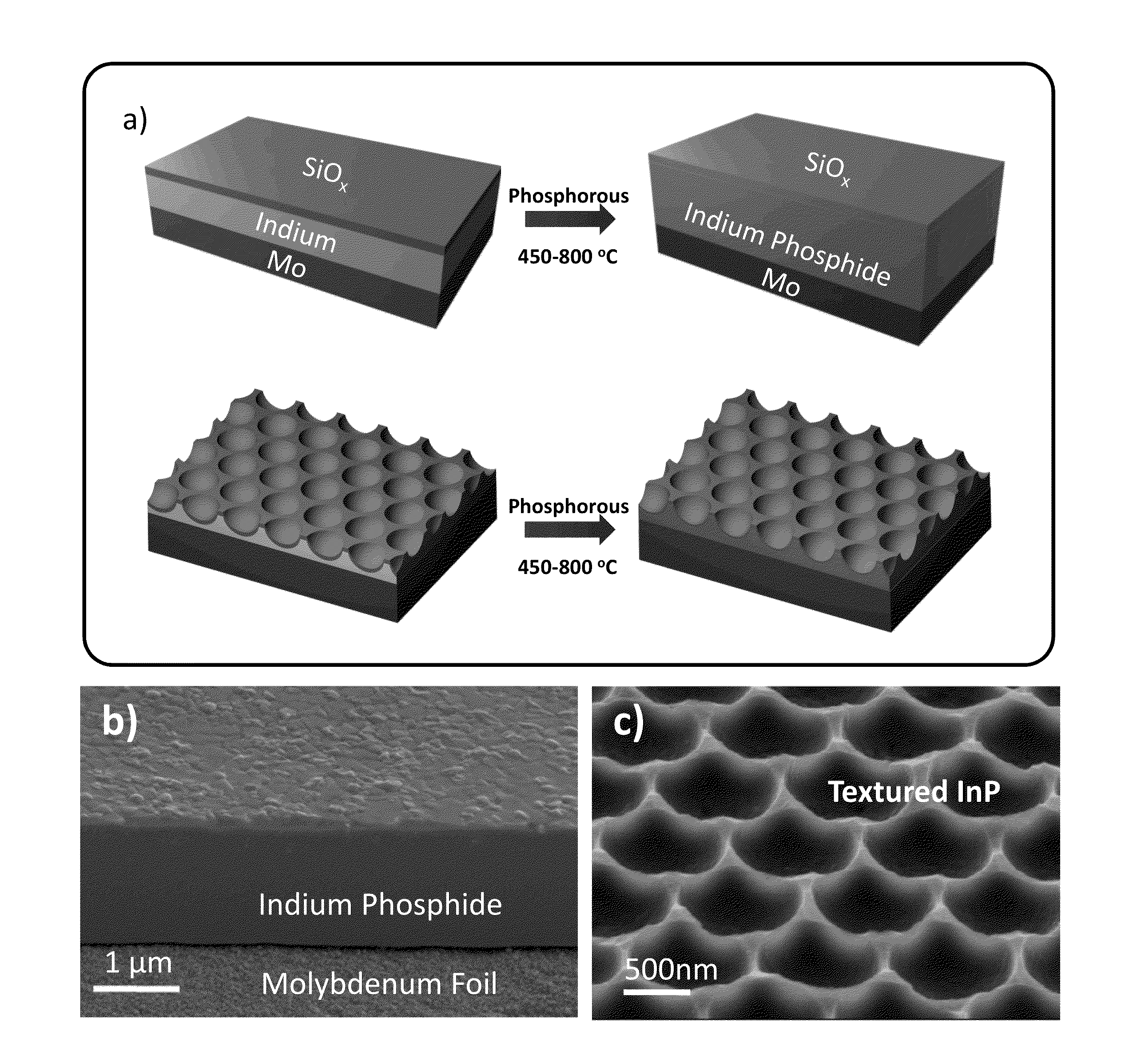
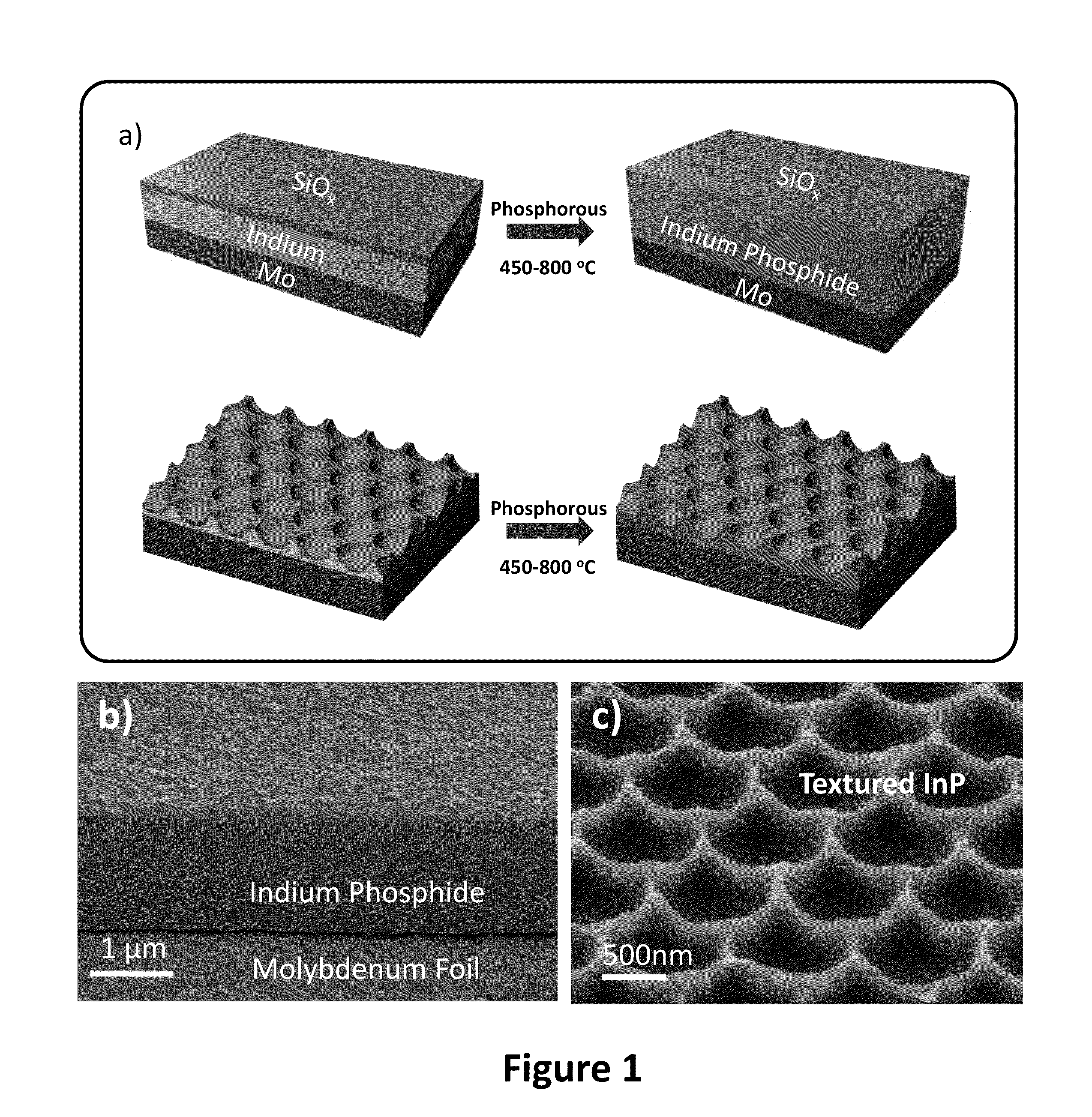
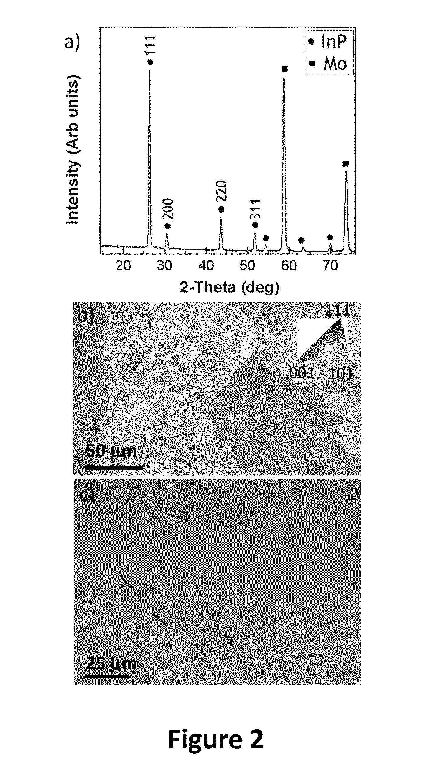
[0019]III-V photovoltaics (PVs) have demonstrated the highest power conversion efficiencies for both single- and multi-junction cells. However, expensive epitaxial growth substrates, low precursor utilization rates, long growth ti...


PUM


Abstract

A composition comprising a substrate, a polycrystalline III-V semiconductor layer, and an oxide layer disposed above the polycrystalline III-V semiconductor layer is described. A growth method that enables fabrication of continuous thin films of polycrystalline indium phosphide (InP) directly on metal foils is described. The method describes the deposition of an indium (In) thin film (up to 20 microns thick) directly on molybedenum (Mo) foil, followed by the deposition of a thin oxide capping layer (up to 1 micron thick). This capping layer prevents dewetting of the In from the substrate during subsequent high temperature processing steps. The Mo/In/Capping Layer stack is then heated in the presence of phosphorous precursors, causing supersaturation of the liquid indium with phosphorous, followed by precipitation of InP. These polycrystalline III-V films have grain sizes 100-200 microns, minority carrier lifetimes >2 ns and hall mobilities of 500 cm̂2/V-s.

Description

CROSS REFERENCE TO RELATED APPLICATIONS[0001]This United States Patent Application claims priority to U.S. Provisional Application Ser. No. 61 / 807,688 filed Apr. 2, 2013, and U.S. Provisional Application Ser. No. 61 / 886,546 filed Oct. 3, 2013,which applications are incorporated herein by reference as if fully set forth in their entirety.STATEMENT OF GOVERNMENTAL SUPPORT[0002]The invention described and claimed herein was made in part utilizing funds supplied by the U.S. Department of Energy under Contract No. DE-AC02-05CH11231 between the U.S. Department of Energy and the Regents of the University of California for the management and operation of the Lawrence Berkeley National Laboratory. The government has certain rights in this invention.BACKGROUND OF THE INVENTION[0003]1. Field of the Invention[0004]The present invention relates to the field of Photovoltaic materials and devices.[0005]2. Related Art[0006]Photovoltaic devices fabricated from III-V semiconductors offer the highest ...

Claims


Application Information

Patent Timeline
IPC IPC(8): H01L31/0368H01L31/0304H01L31/18
CPCH01L31/0368H01L31/0304H01L31/184H01L31/1852Y02E10/544Y02P70/50
Inventor JAVEY, ALIYU, ZHIBINKAPADIA, REHAN
Owner RGT UNIV OF CALIFORNIA
Why Eureka
Try Eureka