Ceramic electronic component and glass paste

Active Publication Date: 2014-10-02
MURATA MFG CO LTD
View PDF4 Cites 23 Cited by
  • Summary
  • Abstract
  • Description
  • Claims
  • Application Information

AI Technical Summary

Benefits of technology

[0011]Accordingly, preferred embodiments of the present invention provide a ceramic electronic compon

Problems solved by technology

However, since the conductive paste used when such a sintered metal film is formed has high viscosity, the sintered metal film has a large thickness.
A plating solution enters the ceramic body through a portion in which the reaction layer has been formed, which poses problems in that the mechanical strength of the ceramic body decreases and the moisture resistance degrades.
Furthermore, an excessively high baking temperature poses a problem in that glass floating occurs through precipitation of a glass component on the surface of the sintered metal film and consequently a plating film is not easily formed on the surface of the sintered metal film.
Therefore, problems such as a decrease in mechanical strength and a degradation of moisture resistance caused by formation of

Method used


Image

  • Ceramic electronic component and glass paste
  • Ceramic electronic component and glass paste
  • Ceramic electronic component and glass paste

Examples


first preferred embodiment

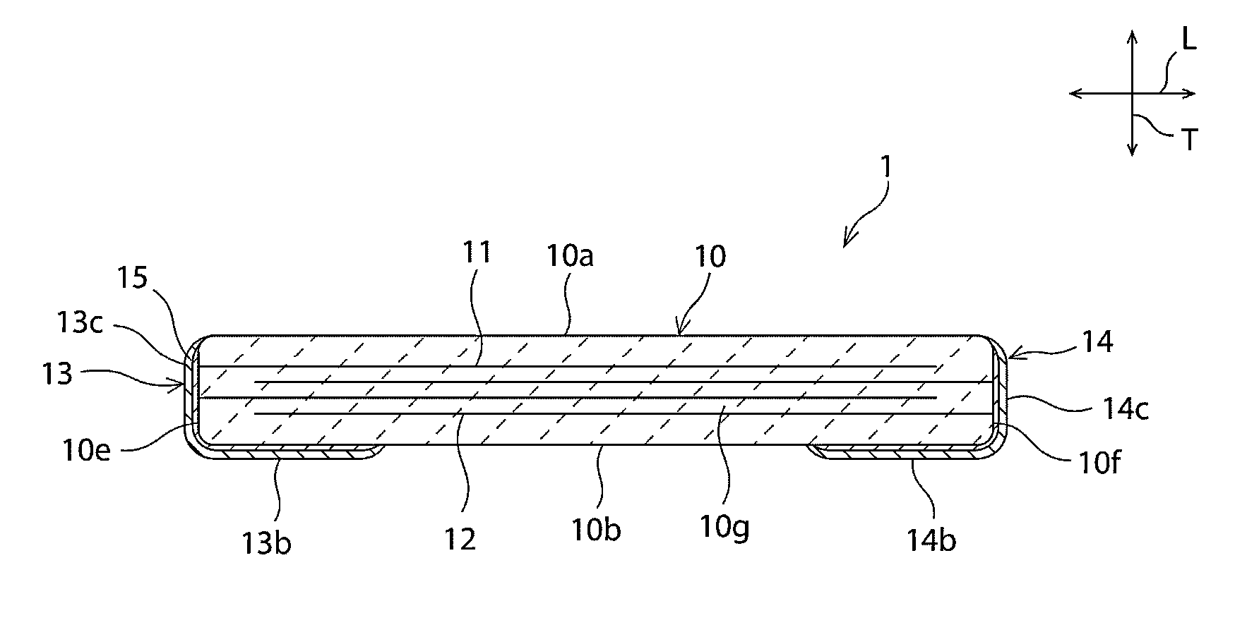
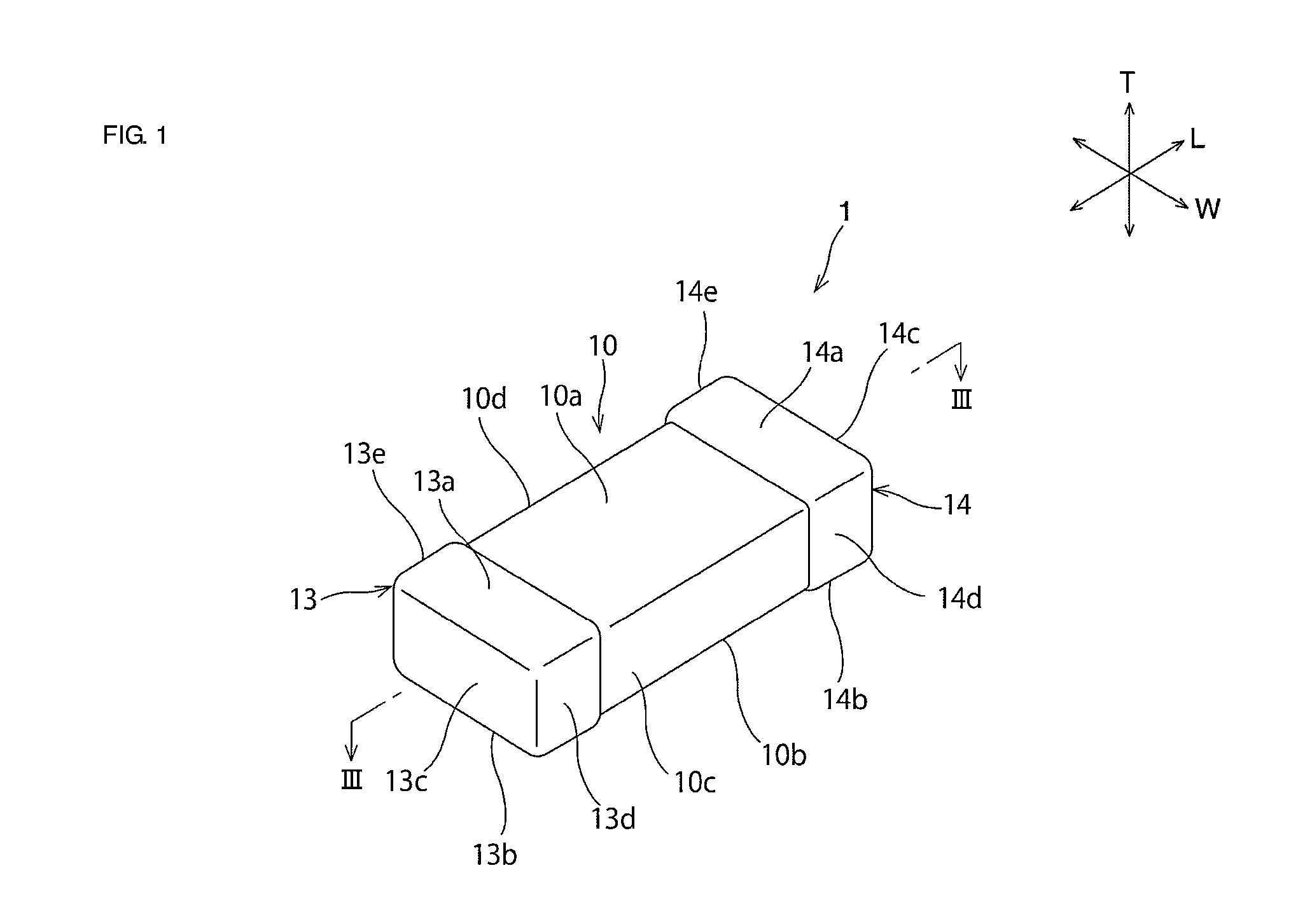
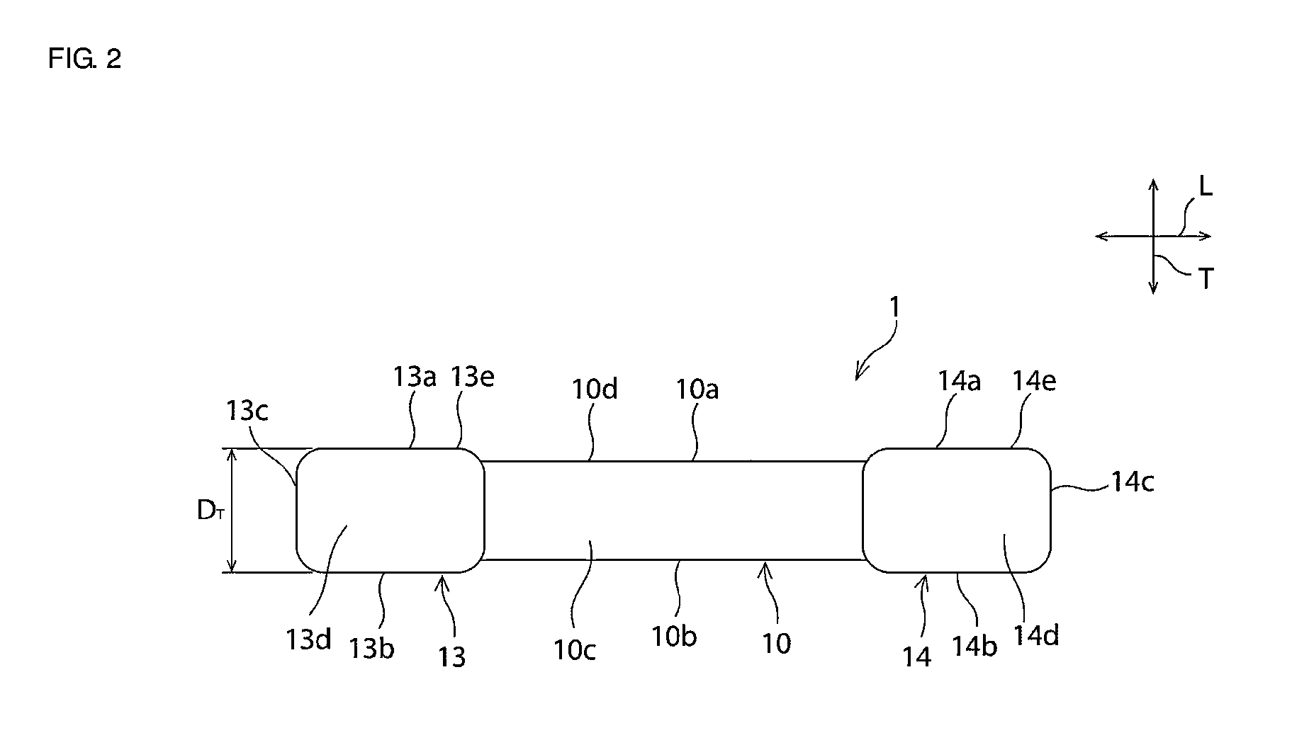
[0042]FIG. 1 is a schematic perspective view of a ceramic electronic component according to the first preferred embodiment of the present invention. FIG. 2 is a schematic side view of the ceramic electronic component according to this preferred embodiment. FIG. 3 is a schematic sectional view taken along line III-III of FIG. 1. FIG. 4 is a schematic sectional view in which a portion enclosed with line IV of FIG. 3 is enlarged. FIG. 5 is a schematic sectional view showing a glass coating layer and a first terminal electrode of a ceramic electronic component produced in this preferred embodiment. FIG. 7 is a schematic sectional view taken along line VII-VII of FIG. 3.

[0043]A structure of a ceramic electronic component 1 will be described with reference to FIGS. 1 to 7.

[0044]As illustrated in FIGS. 1 to 3 and 7, the ceramic electronic component 1 includes a ceramic body 10. The ceramic body 10 is composed of an appropriate ceramic material that provides the functions of the ceramic ele...

second preferred embodiment

[0116]FIG. 11 is a schematic perspective view of a ceramic electronic component according to a second preferred embodiment of the present invention.

[0117]In the first preferred embodiment, an example in which the first and second terminal electrodes 13 and 14 and the glass coating layers 15 are located on the first and second side surfaces 10c and 10d has been described. However, as illustrated in FIG. 11, the first and second terminal electrodes 13 and 14 and the glass coating layers 15 are not necessarily formed on the first and second side surfaces 10c and 10d, for example.

[0118]The ceramic electronic component according to the second preferred embodiment can be produced by, for example, the following method. A mother multilayer body 22 (refer to FIG. 12) is obtained in the same manner as the method for producing the ceramic electronic component 1 according to the first preferred embodiment. In this preferred embodiment, as illustrated in FIG. 12, a conductive pattern 23 having a...

third preferred embodiment

[0121]FIG. 13 is a schematic sectional view of a ceramic electronic component according to a third preferred embodiment of the present invention.

[0122]In the first preferred embodiment, an example in which the first and second terminal electrodes 13 and 14 and the glass coating layers 15 are provided on the first and second principal surfaces 10a and 10b has been described. However, the present invention is not limited to the structure. The first and second terminal electrodes 13 and 14 and the glass coating layers 15 may each be provided in any portion on the surface of the ceramic body 10.

[0123]For example, as illustrated in FIG. 13, the first and second terminal electrodes 13 and 14 and the glass coating layers 15 may be provided on only the second principal surface 10b among the first and second principal surfaces 10a and 10b.


PUM

PropertyMeasurementUnit
Thicknessaaaaaaaaaa
Thicknessaaaaaaaaaa
Percent by volumeaaaaaaaaaa

Abstract

A ceramic electronic component includes a ceramic body, a glass coating layer, and terminal electrodes. End portions of inner electrodes are exposed at a surface of the ceramic body. The glass coating layer covers portions of the ceramic body in which the inner electrodes are exposed. The terminal electrodes are disposed directly above the glass coating layer and are each constituted by a plating film. The glass coating layer includes a glass medium and metal powder particles that are dispersed in the glass medium and define conductive paths which electrically connect the inner electrodes and the terminal electrodes. The metal powder particles include first metal powder particles and second metal powder particles. The first metal powder particles are flat or substantially flat powder particles. The second metal powder particles are spherical or substantially spherical powder particles.

Description

BACKGROUND OF THE INVENTION[0001]1. Field of the Invention[0002]The present invention relates to a ceramic electronic component and a glass paste.[0003]2. Description of the Related Art[0004]Hitherto, ceramic electronic components such as ceramic capacitors have been used for electronic devices such as cellular phones and portable music players. Ceramic electronic components generally include a ceramic body having a surface at which an end portion of each of inner electrodes is exposed and outer electrodes disposed so as to cover a portion of the ceramic body in which the inner electrode is exposed. Examples of the outer electrodes include outer electrodes obtained by applying and baking a conductive paste to form a sintered metal film and plating the sintered metal film as disclosed in Japanese Unexamined Patent Application Publication No. 2002-203737 and outer electrodes formed only of a plating film as disclosed in Japanese Unexamined Patent Application Publication No. 2004-32798...

Claims


Application Information

Patent Timeline
IPC IPC(8): C03C8/18H01L41/083H01C7/00H01G4/30H01F27/28
CPCC03C8/18H01G4/30H01L41/083H01C7/008H01F27/2804H10N30/871H10N30/883H01G4/232H01G4/228
Inventor NISHISAKA, YASUHIROMATSUNO, SATOSHIKISUMI, TETSUYAOKABE, YOKO
Owner MURATA MFG CO LTD
Why Eureka
Try Eureka