Method for measuring film thickness distribution

Active Publication Date: 2014-10-02
SHIN-ETSU HANDOTAI CO LTD
View PDF10 Cites 19 Cited by
  • Summary
  • Abstract
  • Description
  • Claims
  • Application Information

AI Technical Summary

Benefits of technology

[0028]In the present invention, since a waveband including a wavelength λ1 observed when the above-described profile P31 of the difference becomes zero, a wavelength λ2 observed when the profile P32 of the difference becomes zero, or both of these wavelengths is selected as the waveband of a light being measured in the film thickness distribution measurement by the reflection spectroscopy and a film thickness distribution is measured,

Problems solved by technology
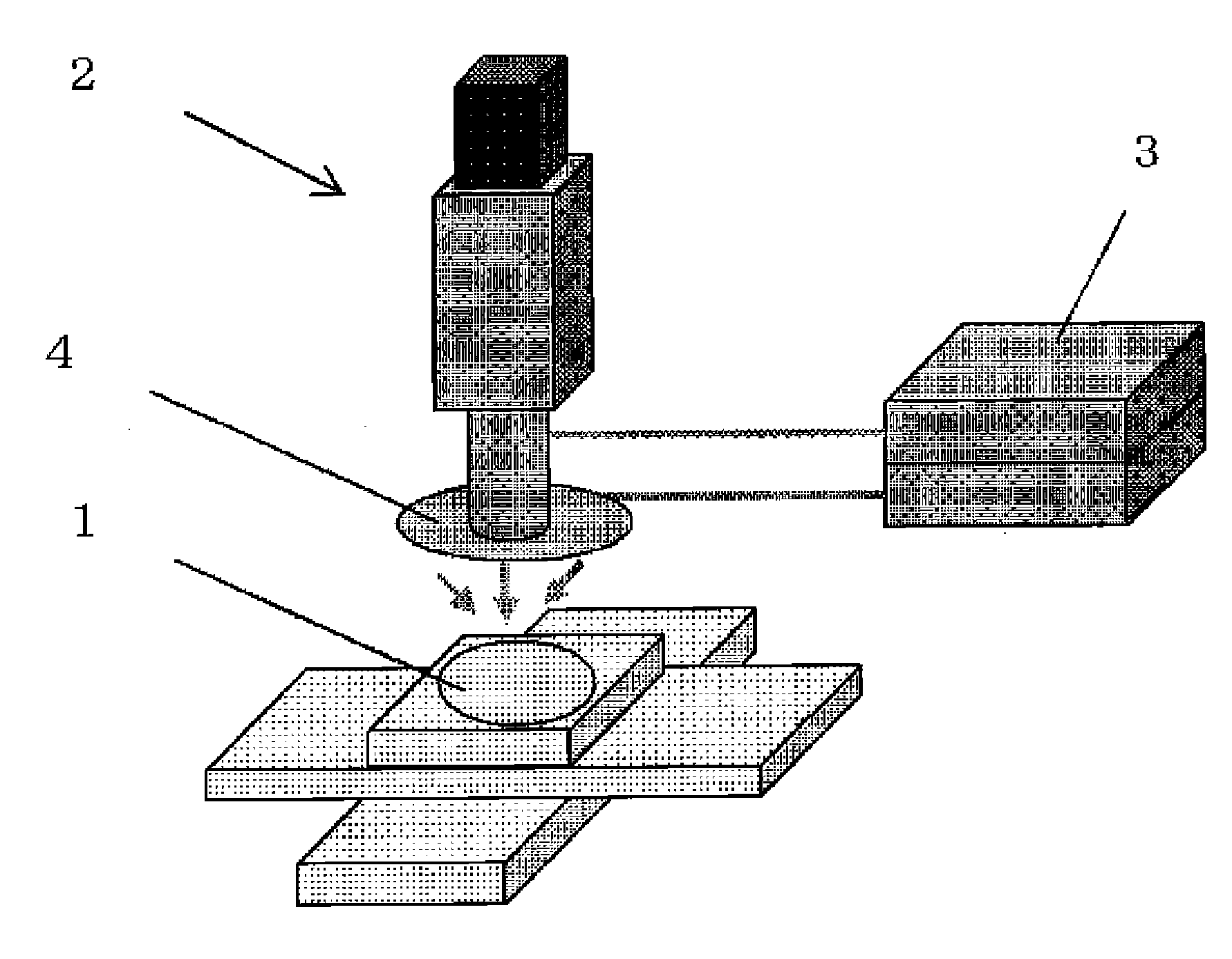
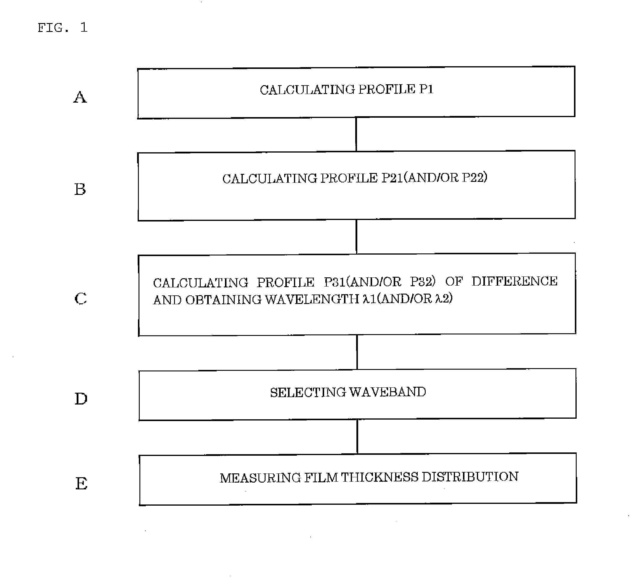
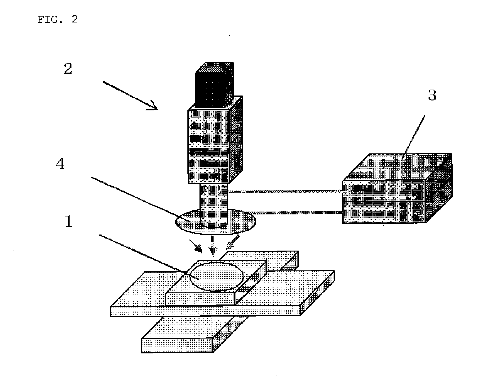
An conventional method for measuring film thickness distribution that calculates the film thickness distribution of a thin film of such a wafer with a thin film, the wafer with a substrate having a thin film on the surface thereof, generally performs film thickness measurement in each point by spectroscopic ellipsometry or reflection spectroscopy, but a film thickness distribution measurement unit that can perform high-throughput, high-precision film thickness distribution measurement on the whole surface of the wafer has not b

Method used


Image

  • Method for measuring film thickness distribution
  • Method for measuring film thickness distribution
  • Method for measuring film thickness distribution

Examples


example 1

[0080]The film thickness distribution of the buried oxide film (a BOX layer) of a 300-mm-diameter SOI wafer was measured by the inventive method depicted in FIG. 1 to evaluate the fitting precision.

[0081]Here, the SOI wafer, an object to be measured, included an SOI layer having a set film thickness of 12 nm and a buried oxide film having a set film thickness of 25 nm. The conditions of the film thickness distribution measurement by the reflection spectroscopy included measurement points on the entire wafer surface at intervals of 1 mm except for a peripheral region of 3 mm. Incidentally, fitting precision is measurement precision based on a 95% confidence interval.

[0082]Profiles P1, P21, and P31 were calculated to select a waveband used for the film thickness distribution measurement by the reflection spectroscopy. In the calculation of P21, the condition of t was that the thickness was increased by 1 nm (the set film thickness of the SOI layer was 13 nm.) The calculated P1 and P21...

example 2

[0085]The film thickness distribution of the SOI layer of an SOI wafer having the same conditions as those of Example 1 was measured by the inventive method depicted in FIG. 1 to evaluate the fitting precision.

[0086]Profiles P1, P22, and P32 were calculated to select a waveband used for the film thickness distribution measurement by the reflection spectroscopy. In the calculation of P22, the condition of t was that the thickness was increased by 1 nm (the set film thickness of the buried oxide film was 26 nm.) The calculated P1 is depicted in FIG. 3A, the calculated P22 is depicted in FIG. 3B, and the calculated P32 is depicted in FIG. 3C. The wavelength λ2 observed when the profile P32 became zero was 535 nm and the selected waveband including the wavelength λ2 was a waveband of 525 to 545 nm.

[0087]The film thickness distribution of the buried oxide film was then measured by the reflection spectroscopy in a manner that the SOI wafer being measured was irradiated with a visible ligh...

example 3

[0089]The film thickness distribution of the SOI layer and the buried oxide film of an SOI wafer having the same conditions as those of Example 1 was measured by the inventive method depicted in FIG. 1 to evaluate the fitting precision.

[0090]Profiles P1, P21, P22, P31 and P32 were calculated to select a waveband used for the film thickness distribution measurement by the reflection spectroscopy. In the calculation of P21, the condition of t was that the thickness was increased by 1 nm (the set film thickness of the SOI layer was 13 nm.) In the calculation of P22, the condition of t was that the thickness was increased by 1 nm (the set film thickness of the buried oxide film was 26 nm.) The calculated P1 and P21 are depicted in FIG. 3A, the calculated P22 is depicted in FIG. 3B, and the calculated P31 and P32 are depicted in FIG. 3C. The wavelengths λ1 and λ2 observed when the profiles P31 and P32 became zero were 608 nm and 535 nm, respectively, and the selected waveband including t...


PUM


Abstract

A method for measuring film thickness distribution, including calculating profile P1 indicating wavelength dependence of a reflectance of a first wafer being an object measured with respect to a light at wavelengths not less than a wavelength region of visible light; calculating profile P21 indicating wavelength dependence of a reflectance of a second wafer to light at wavelengths not less than wavelength region of visible light; obtaining a wavelength λ1 observed when profile P31 of a difference between calculated profiles P1 and P21 becomes zero; and selecting waveband including the obtained wavelength λ1 as a waveband of light for use in film thickness distribution measurement by reflection spectroscopy. The film thickness distribution of the first thin film is measured by reflection spectroscopy in a manner that a surface of the first wafer is irradiated with a light to selectively measure only reflected light at a selected waveband.

Description

TECHNICAL FIELD[0001]The present invention relates to a method for measuring film thickness distribution of wafers with two layers of thin films for use in semiconductor devices by reflection spectroscopy.BACKGROUND ART[0002]In recent years, with miniaturization of a design rule, SOI wafers, each having an ultrathin film (i.e., an ultrathin SOI layer) which needs to be particularly high uniform, are used for SOI devices, such as FD-SOI (Fully Depleted SOI) devices, FinFET devices, and Si nanowire transistors. In these devices, the uniformity of SOI film thicknesses and buried oxide film (BOX film) thicknesses is important to determine the characteristics of transistors.[0003]An conventional method for measuring film thickness distribution that calculates the film thickness distribution of a thin film of such a wafer with a thin film, the wafer with a substrate having a thin film on the surface thereof, generally performs film thickness measurement in each point by spectroscopic elli...

Claims


Application Information

Patent Timeline
IPC IPC(8): G01B11/06
CPCG01B2210/56G01B11/0633G01B11/0625H01L22/12H01L2924/0002H01L2924/00G01B11/06
Inventor KUWABARA, SUSUMU
Owner SHIN-ETSU HANDOTAI CO LTD
Why Eureka
Try Eureka