Substrate mounting table and plasma treatment device
Inactive Publication Date: 2014-10-23
TOKYO ELECTRON LTD
View PDF10 Cites 21 Cited by
- Summary
- Abstract
- Description
- Claims
- Application Information
AI Technical Summary
Benefits of technology
The patent aims to achieve uniformity in the depth of holes in a substrate. This can be achieved using various techniques described in the patent.
Problems solved by technology
When the etching processing is continuously performed, a deviation in temperature distribution in a wafer plane may be further significant due to heat input from plasma.
In this case, the uniformity in etching rate in the wafer plane or the uniformity in hole depth in the wafer plane may be impaired, and also it may become difficult to realize a vertical hole shape.
Method used
View moreImage
Smart ImageViewing Examples

Examples
example 1
[0164]The diameter of the supporting surface 6e was 302 mm. As the wafer W, a silicon wafer was used.
example 2
[0165]The diameter of the supporting surface 6e was 302 mm. As the wafer W, a quartz wafer was used.
example 3
[0172]The diameter of the supporting surface 6e was 302 mm.
Login to View More PUM
| Property | Measurement | Unit |
|---|---|---|
| Diameter | aaaaa | aaaaa |
| Diameter | aaaaa | aaaaa |
| Length | aaaaa | aaaaa |
Abstract
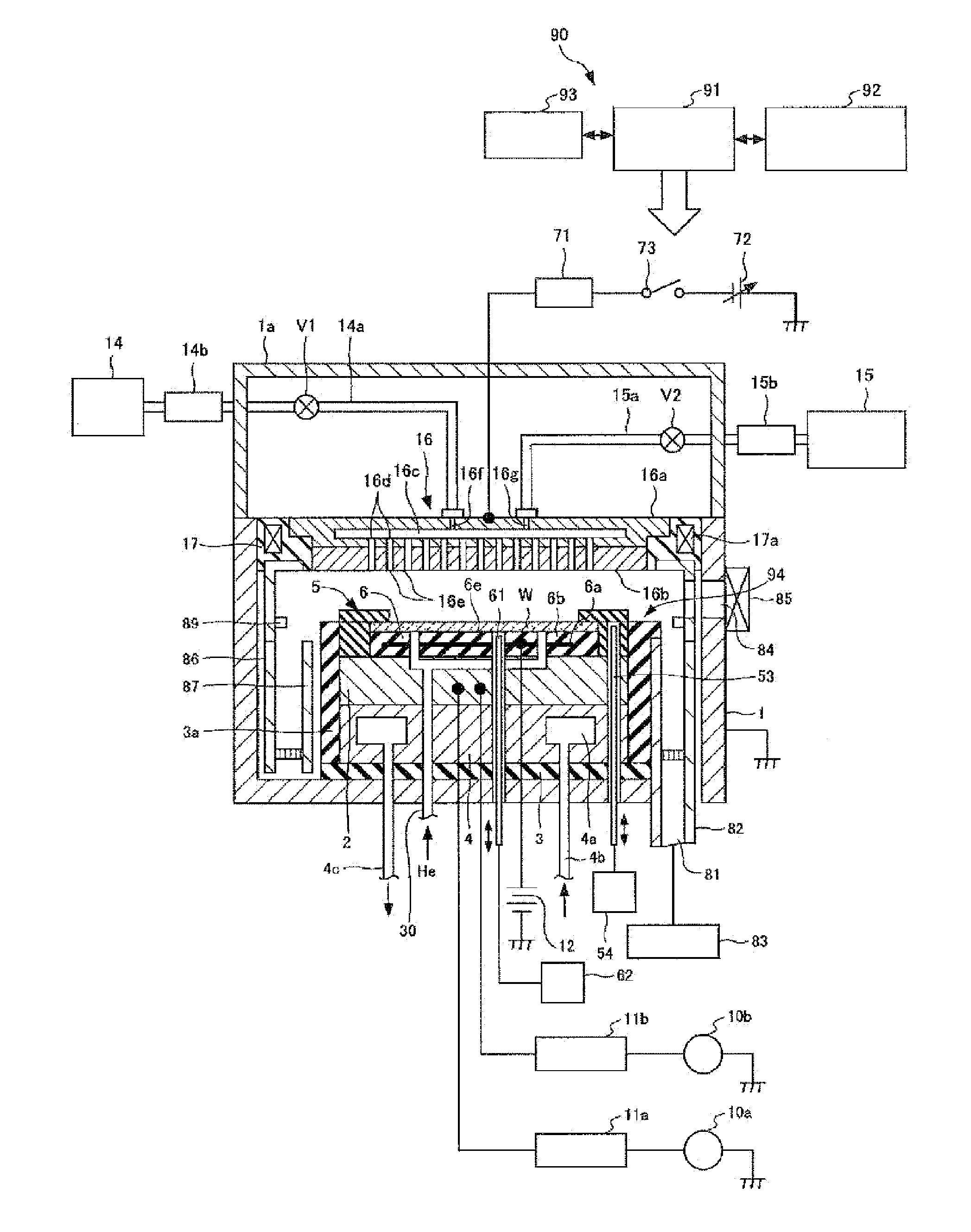
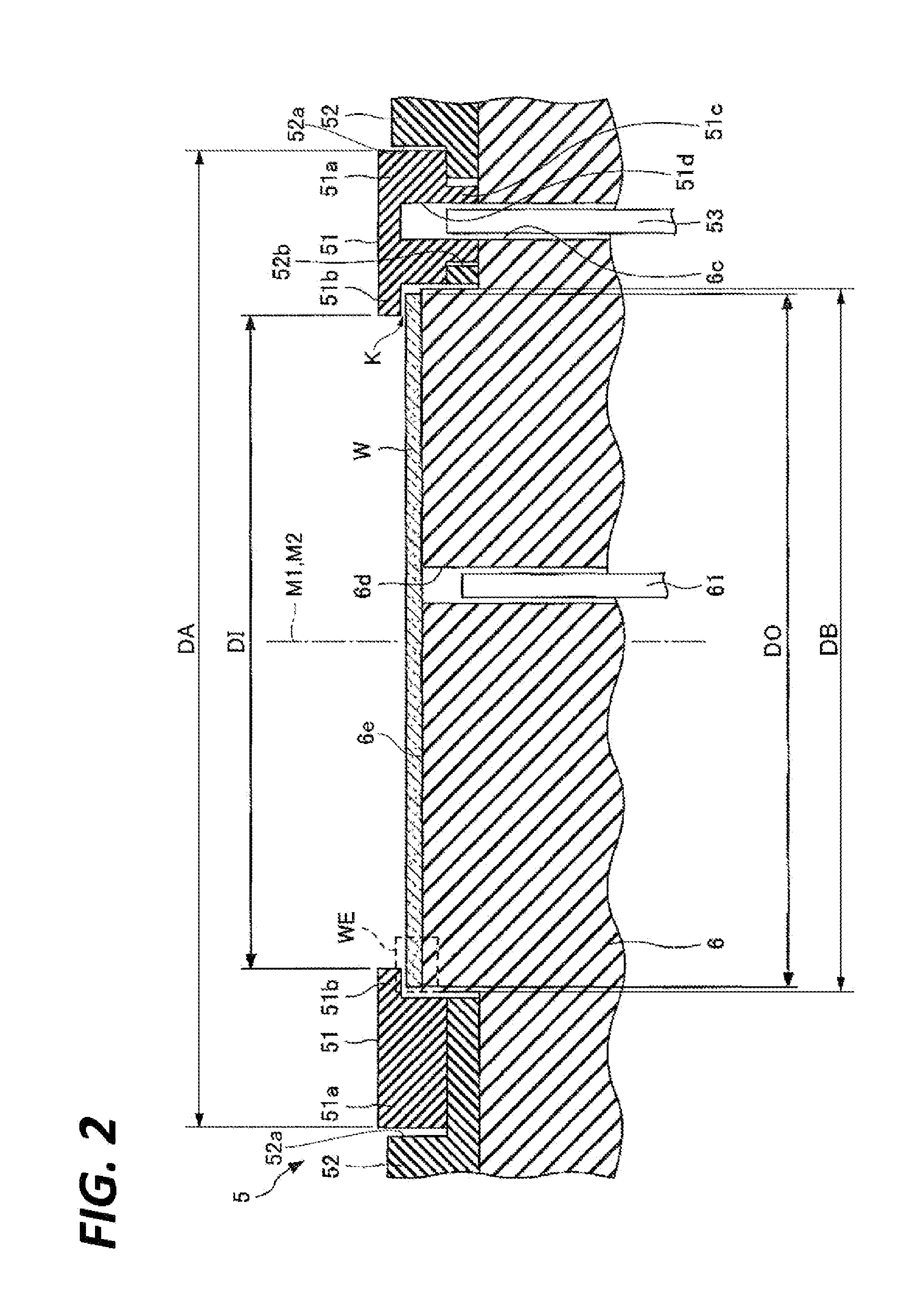
A substrate mounting table (94) is equipped with a mounting table (2), an electrostatic chuck (6), and a bevel covering (5). The electrostatic chuck (6) has a supporting surface (6e) which is in contact with the whole of the rear surface of a wafer (W). The annular bevel covering (5) has an outer diameter (DA) which is greater than that of the supporting surface (6e), and an inner diameter (DI) which is smaller than that of the wafer (W). The bevel covering (5) is disposed such that, when viewed from the direction orthogonal to the supporting surface (6e), the bevel covering (5) surrounds the periphery of the wafer (W) supported on the supporting surface (6e).
Description
TECHNICAL FIELD[0001]The present disclosure relates to a substrate mounting table and a plasma treatment device.BACKGROUND ART[0002]In a plasma treatment device, a ring-shaped member called a focus ring may be disposed to surround the periphery of a wafer as a substrate to be processed (see, e.g., Patent Document 1). The focus ring disclosed in Patent Document 1 is disposed around a substrate mounting table provided with a substrate supporting unit which has a supporting surface configured to support the wafer. The supporting surface has a diameter slightly smaller than a diameter of the wafer. Since the focus ring is provided, plasma may be confined, and discontinuity of a bias potential due to an edge surface effect is reduced in a wafer plane so that a uniform and good processing may be performed at the periphery portion of the wafer as well as at the center of the wafer.[0003]However, as disclosed in Patent Document 1, when the top surface of the substrate mounting table is form...
Claims
Login to View More Application Information
Patent Timeline
 IPC IPC(8): H01J37/32
CPCH01J37/32715H01L21/3065H01L21/68721H01L21/68735H01L21/76898H01L21/31138H01L21/6835H01L2221/68327H01L2221/6834H01L2221/68386
Inventor HATOH, HIDEYUKIDOBA, SHIGEKIYAMAMOTO, SHINYAYAMADA, SATOSHIMORI, HIROTOANDO, KENJI
Owner TOKYO ELECTRON LTD