Electron emitting device
- Summary
- Abstract
- Description
- Claims
- Application Information
AI Technical Summary
Benefits of technology
Problems solved by technology
Method used
Image

Examples
first embodiment
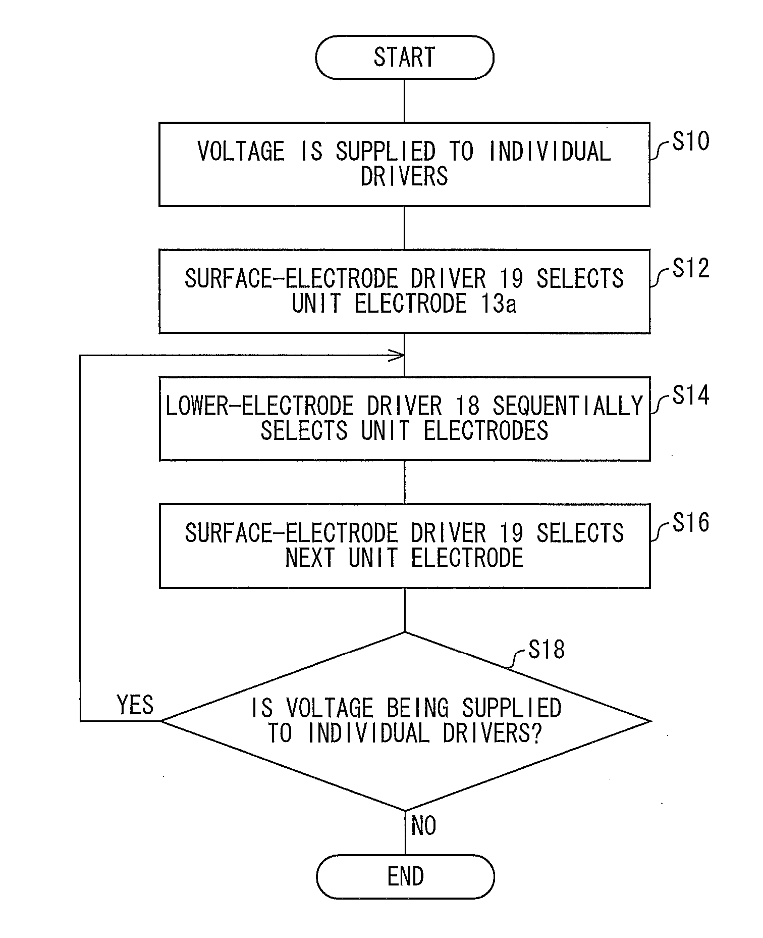
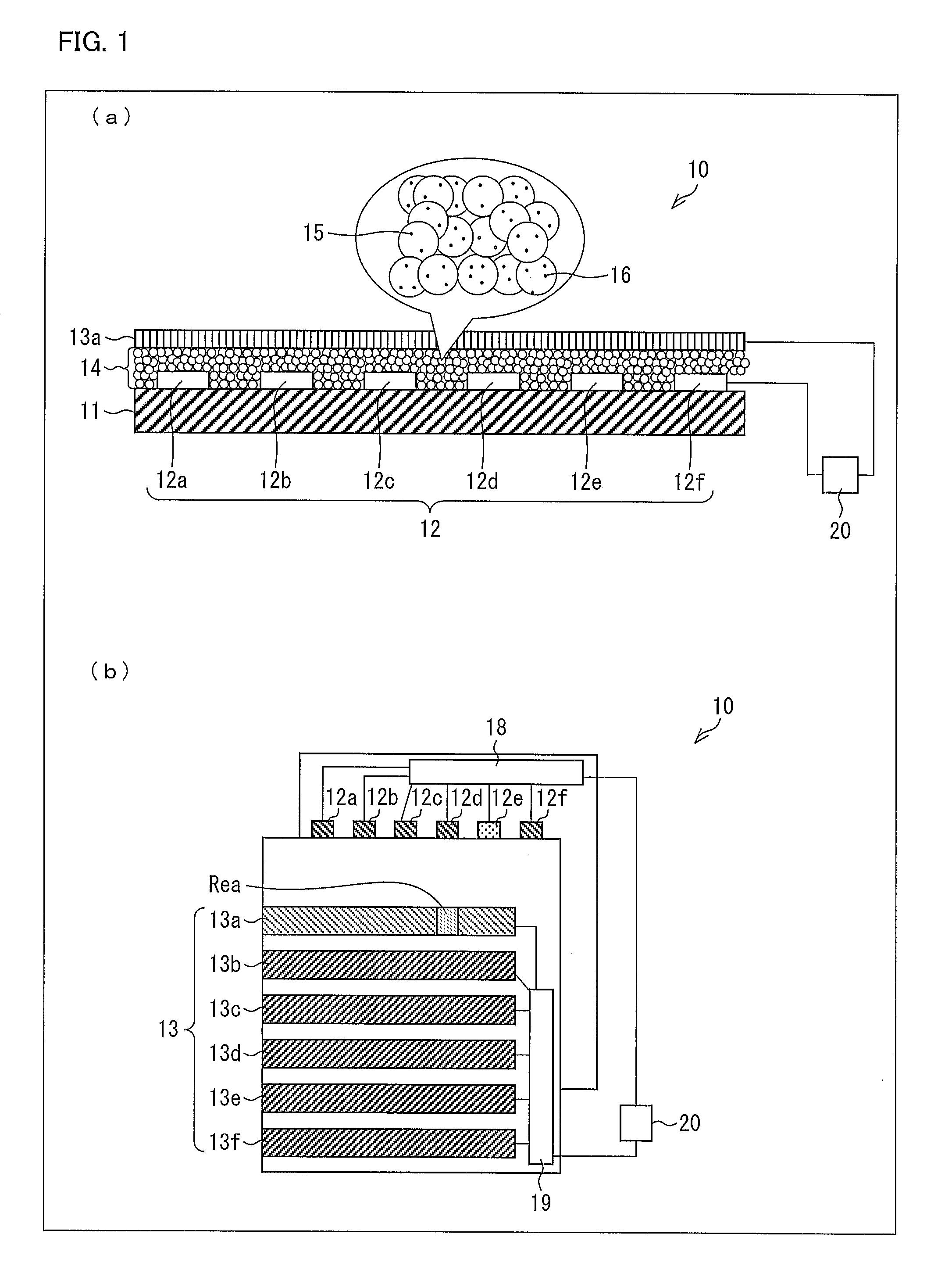
[0025]Hereinafter, an electron emitting device 10 according to a first embodiment will be described with reference to FIGS. 1A to 3. The electron emitting device 10 constitutes, together with a power supply 20 serving as a power supply unit, an electron emitting apparatus 1 according to an embodiment of the present disclosure. In the electron emitting device 10, a voltage supplied from the power supply 20 is applied between a lower electrode and a surface electrode to accelerate electrons between the lower electrode and the surface electrode, so that the electrons are emitted from the surface electrode.
Overview of Electron Emitting Device 10
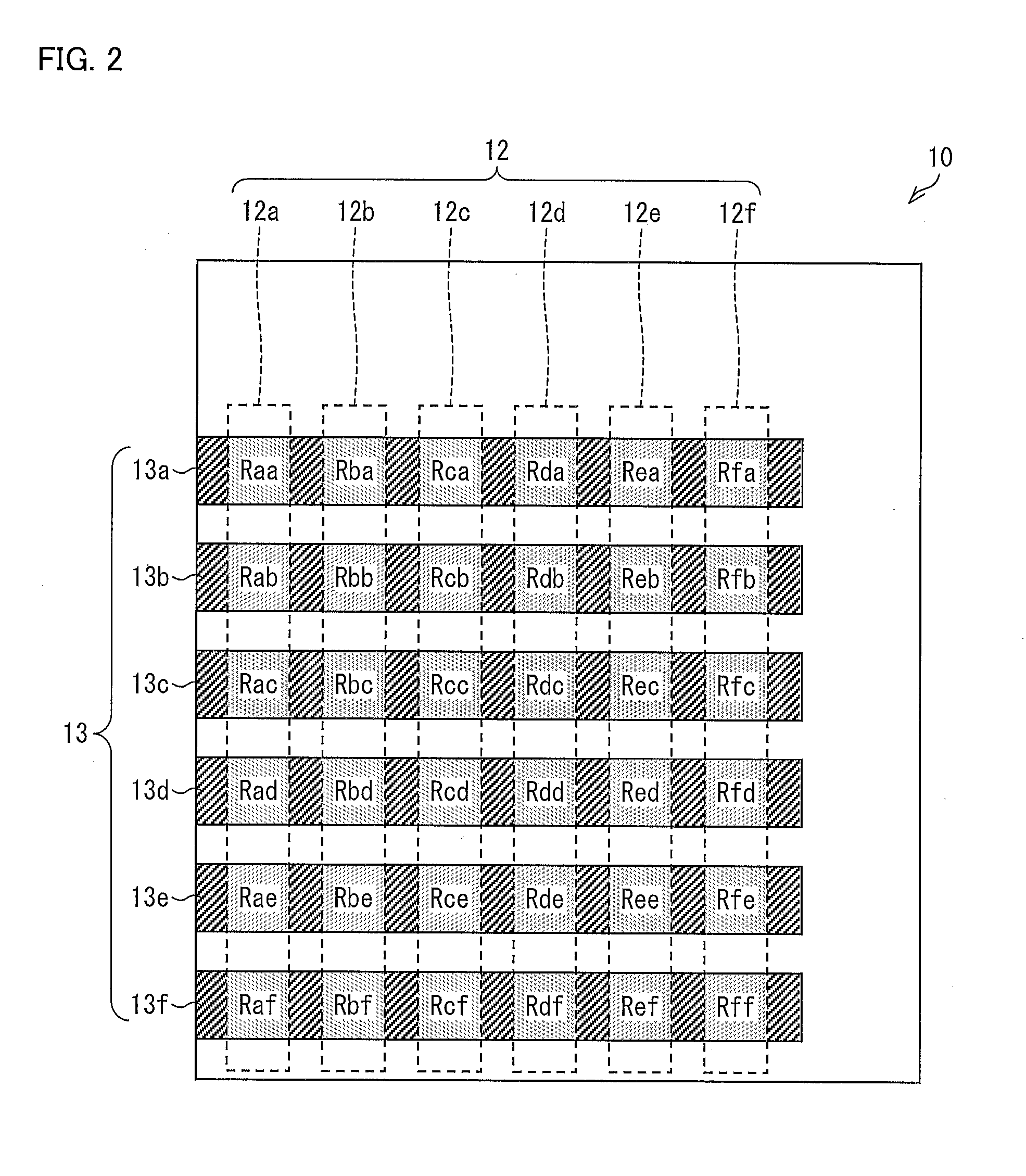
[0026]FIGS. 1A and 1B are diagrams illustrating a schematic configuration of the electron emitting device 10. FIG. 1A is a cross-sectional view of the electron emitting device 10, more specifically, is a cross-sectional view taken along a straight line that is parallel to the longitudinal direction of unit electrodes included in a surface electro...
second embodiment
[0070]Hereinafter, the electron emitting device 30 according to a second embodiment will be described with reference to FIG. 4. For the convenience of description, the parts having the same functions as those described in the first embodiment are denoted by the same reference numerals, and the corresponding description is omitted. FIG. 4 is a top view illustrating a schematic configuration of the electron emitting device 30.
[0071]As illustrated in FIG. 4, the electron emitting device 30 is different from the electron emitting device 10 according to the first embodiment in that a single surface electrode 33 that does not include unit electrodes is provided. The surface electrode 33 is configured to cover the lower electrode 12.
[0072]When the electron emitting device 30 is driven, a voltage is constantly applied to the surface electrode 33 from the power supply 20. On the other hand, the lower-electrode driver 18 sequentially selects, from among the six unit electrodes 12a to 12f, one...
third embodiment
[0077]Hereinafter, an electron emitting device 40 according to a third embodiment will be described with reference to FIGS. 5A and 5B. For the convenience of description, the parts having the same functions as those described in the first embodiment are denoted by the same reference numerals, and the corresponding description is omitted. FIGS. 5A and 5B are diagrams illustrating a schematic configuration of the electron emitting device 40, in which FIG. 5A is a cross-sectional view and FIG. 5B is a top view.
[0078]As illustrated in FIG. 5A, the electron emitting device 40 is different from the electron emitting device 10 according to the first embodiment in that an electron acceleration layer 44 made of a resin containing conductive microparticles (not illustrated) is provided. As illustrated in FIG. 5B, the electron emitting device 40 includes the lower electrode 12 including the unit electrodes 12a to 12f and the surface electrode 13 including the unit electrodes 13a to 13f. The co...
PUM
 Abstract
Description
Claims
Application Information
 - Generate Ideas
- Intellectual Property
- Life Sciences
- Materials
- Tech Scout
- Unparalleled Data Quality
- Higher Quality Content
- 60% Fewer Hallucinations
Browse by: Latest US Patents, China's latest patents, Technical Efficacy Thesaurus, Application Domain, Technology Topic, Popular Technical Reports.
© 2025 PatSnap. All rights reserved.Legal|Privacy policy|Modern Slavery Act Transparency Statement|Sitemap|About US| Contact US: help@patsnap.com