

Ultrasonic wire bonding wedge with multiple bonding wire slots
a technology bonding wire, which is applied in the direction of soldering apparatus, manufacturing tools,auxillary welding devices, etc., can solve the problems of low efficiency of ultrasonic wire bonding operation and useless chips, and achieve the effect of reducing the defective rate of chips, sufficient bonding strength of bonding operation, and improving bonding operation efficiency
- Summary
- Abstract
- Description
- Claims
- Application Information
AI Technical Summary
Benefits of technology
Problems solved by technology
Method used
Image

Examples
Embodiment Construction
[0026]The following detailed description refers to embodiments, which serves as illustrative purpose for describing the technique features of the invention, instead of restriction to the scope of the present invention.
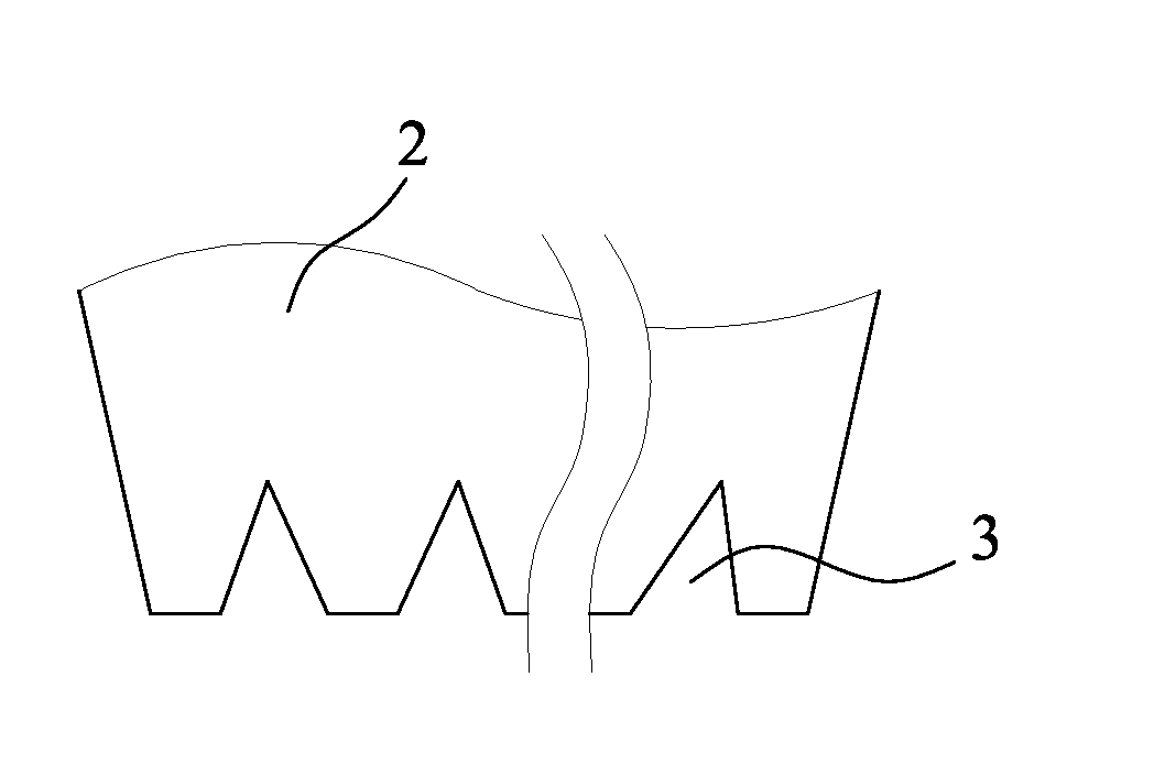
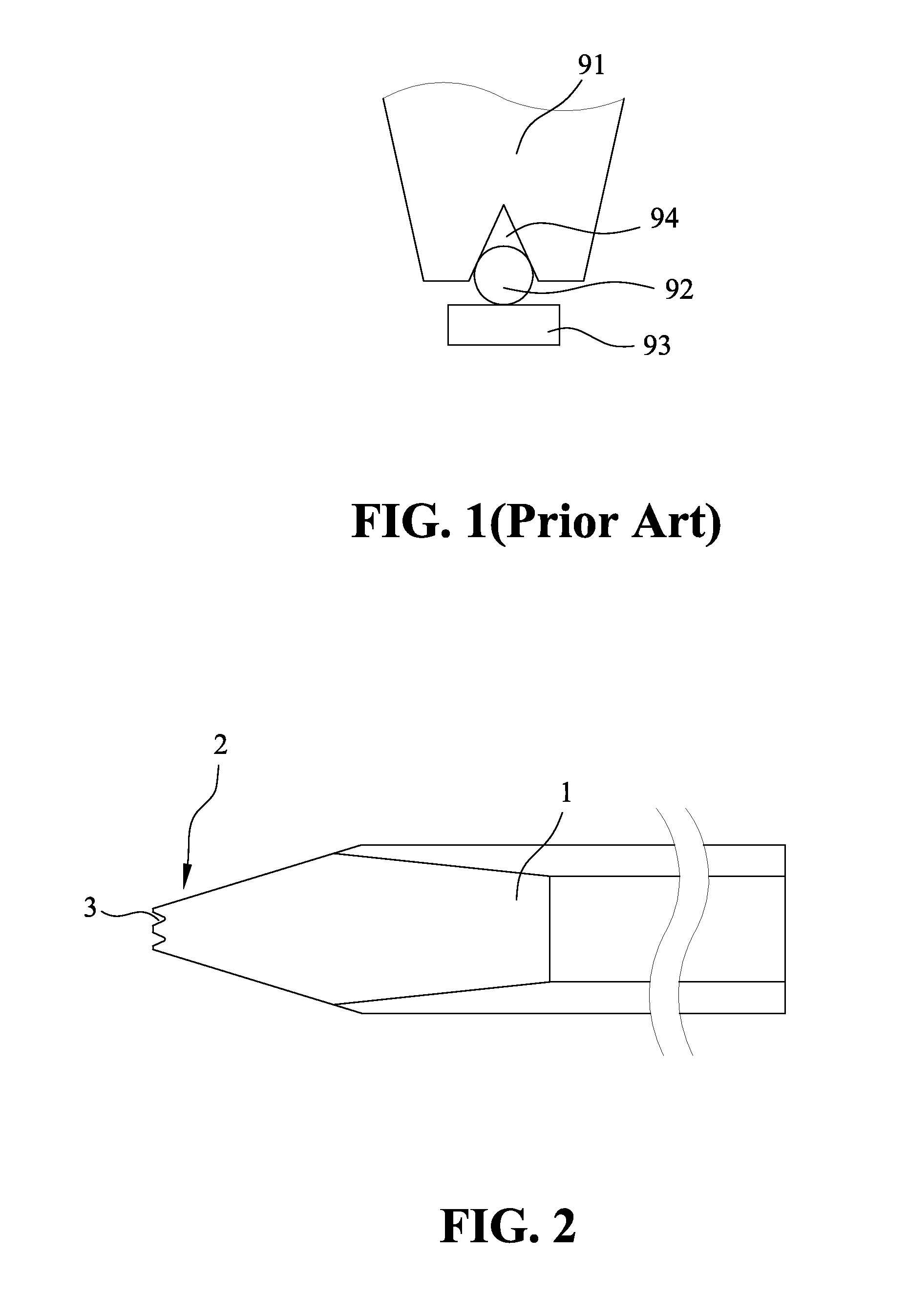
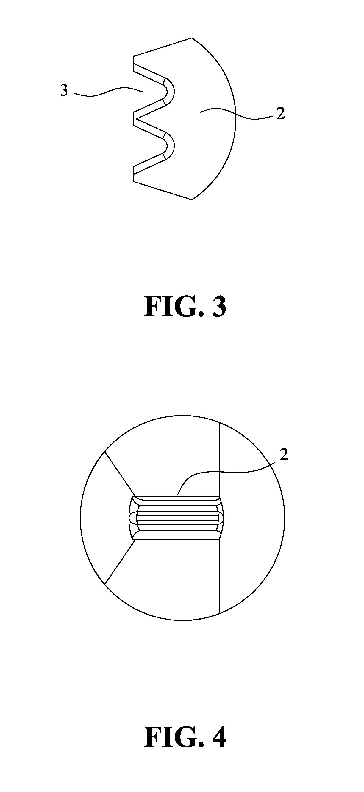
[0027]FIG. 2, FIG. 3 and FIG. 4 show the first embodiment of the present invention. An ultrasonic wire bonding wedge with multiple bonding wire slots includes a pillar fixing part 1 for providing fixed connection to the bonding device. One end of the fixing part includes a wire bonding wedge nozzle 2, with feature that the tip of the nozzle including at least two bonding wire slots 3.
[0028]In the present embodiment, the at least two bonding wire slots are located in the middle area of the wire bonding wedge nozzle. The wire bonding wedge nozzle has a conic structure. The width of the opening of the bonding wire slot is no less than width of any part of the bonding wire slot. In other words, the outermost opening has a largest width of the bonding wire slot 3. The two b...
PUM
| Property | Measurement | Unit |
|---|---|---|
| depth | aaaaa | aaaaa |
| area | aaaaa | aaaaa |
| width | aaaaa | aaaaa |
Abstract
Description
Claims
Application Information