Conductive nanostructure-based films with improved ESD performance

a nanostructure and nano-based technology, applied in the field of optical stacks, can solve the problems of reducing affecting the continuity of all or a portion affecting the continuity of the patterned transparent conductor layer, so as to reduce the risk of electrostatic discharge, reduce the risk of damage, and reduce the area of charge accumulation

Active Publication Date: 2014-11-20
CHAMP GREAT INTL
View PDF5 Cites 11 Cited by
  • Summary
  • Abstract
  • Description
  • Claims
  • Application Information

AI Technical Summary

Benefits of technology

[0009]Grounding an electrode positioned closely proximate to the patterned transparent conductor generally results in less damage to the patterned transparent conductor due to fact that the current is limited by the capacitance provided by the closely proximate electrodes. On the other hand, direct grounding of the patterned transparent conductor causes a larger voltage differential increasing the power dissipated through the patterned transparent conductor.
[0010]The threat of irreparable damage to patterned transparent conductors from electrostatic discharge caused by grounding of the patterned transparent conductors in the production or manufacturing process (e.g., during roll-to-roll production) may be reduced by incorporating one or more anti-static or

Problems solved by technology

In optical stacks containing patterned transparent conductor layers, there exists a risk of an electrostatic discharge causing a current density sufficient to damage portions of the patterned transparent conductor structure.
Thermal damage occurs to the transparent conductor structures subjected to this large current.
At times, the thermal damage is sufficient

Method used


Image

  • Conductive nanostructure-based films with improved ESD performance
  • Conductive nanostructure-based films with improved ESD performance
  • Conductive nanostructure-based films with improved ESD performance

Examples


Embodiment Construction

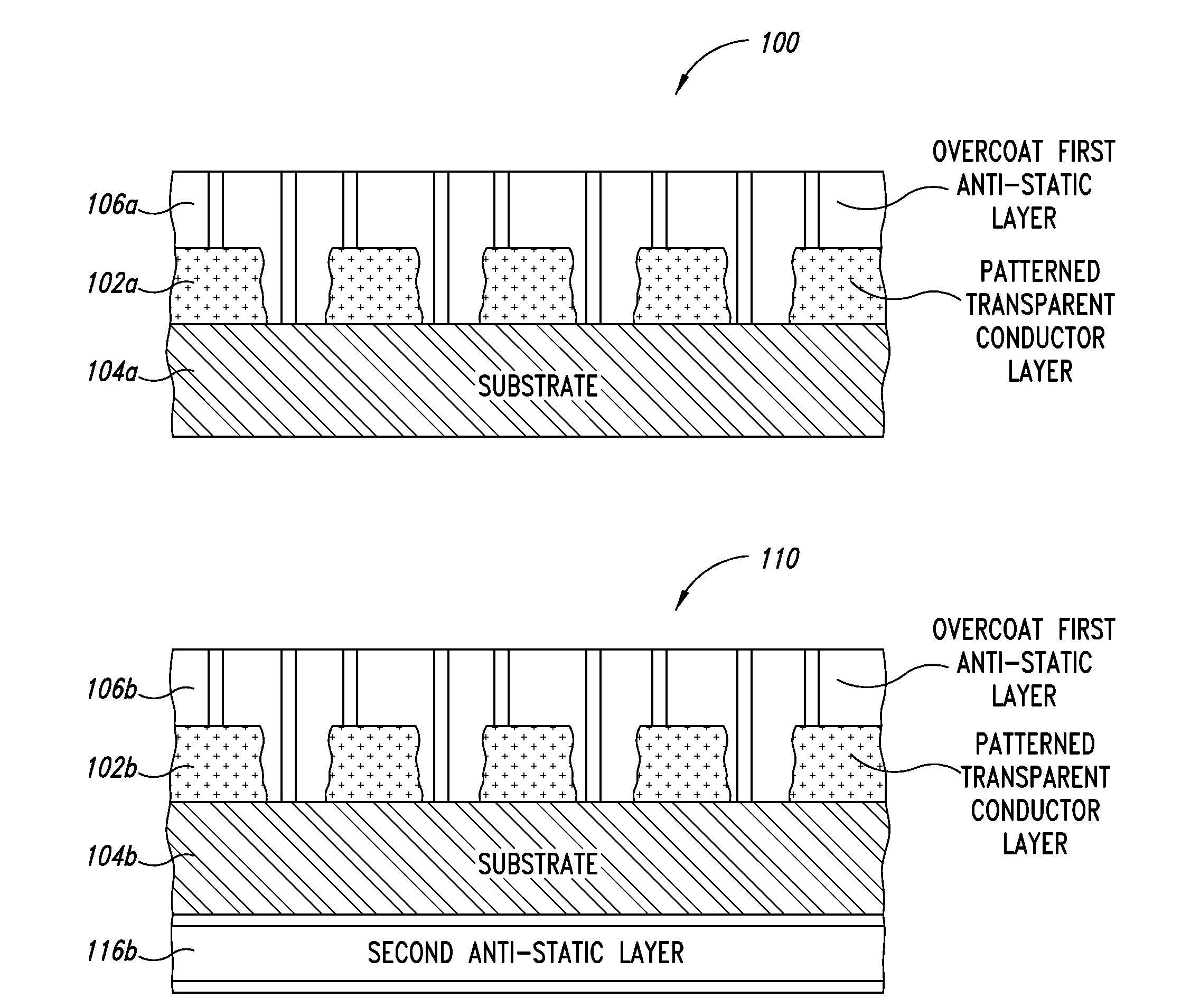
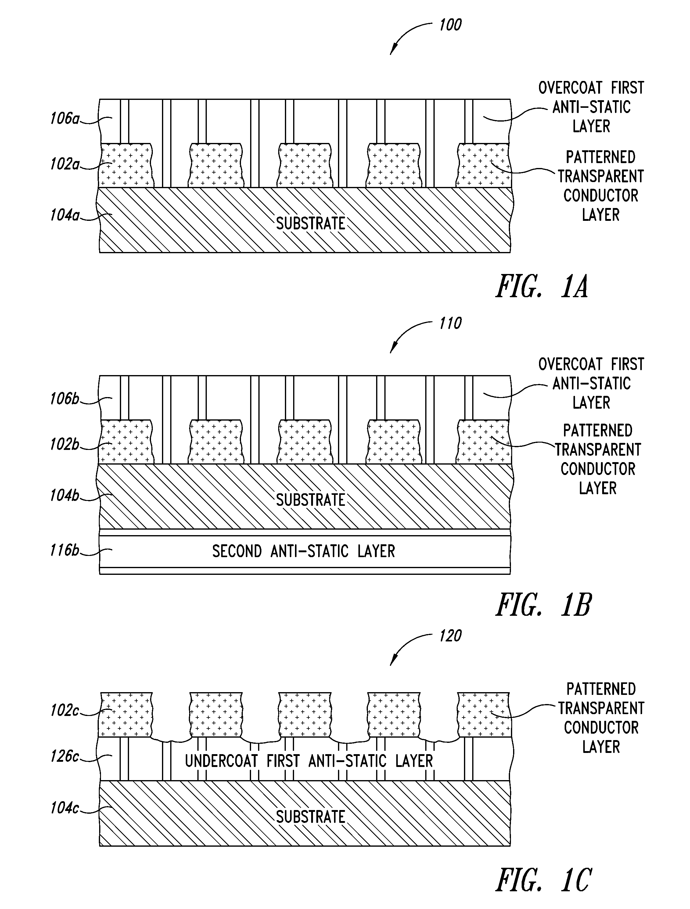
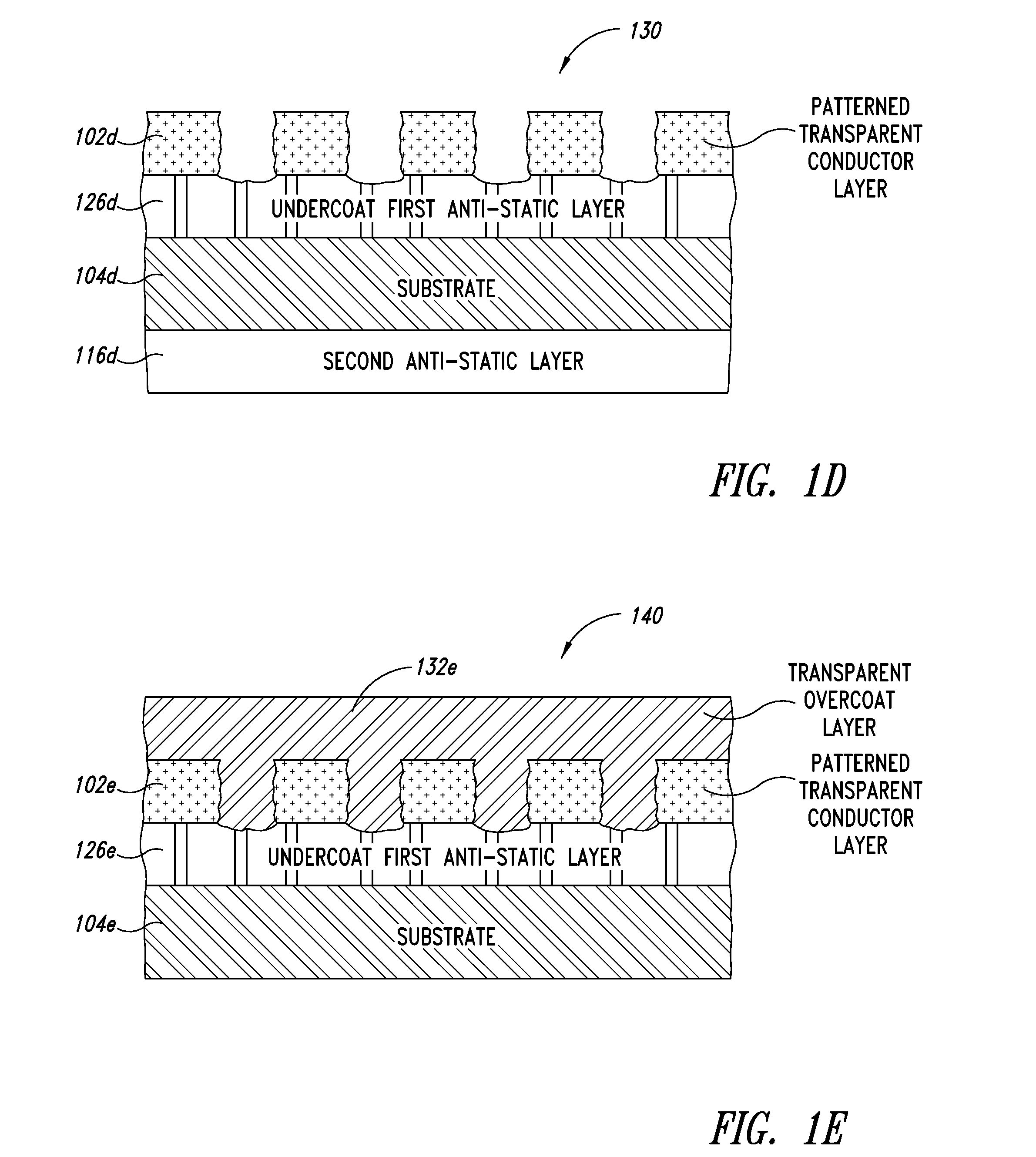
[0031]The optical stacks and methods described herein are presented in the form of various embodiments. It should be understood that variations are possible within each of these embodiments and in other embodiments not specifically described for the sake of clarity and / or to avoid redundancy within this disclosure. Additionally, the order, extent, and composition of the various layers and structures disclosed herein can be varied, altered, divided, or subdivided to meet varying performance specifications.

[0032]The terms top, bottom, left, and right as used herein denote relative and not absolute orientations. Thus a structure that in one embodiment has layer “A” identified as a “top” layer may, in a second embodiment, be inverted such that layer “A” is now identified as a “bottom” layer in the structure. Such re-oriented, repositioned, and / or rotated embodiments are included in the scope of the following disclosure.

[0033]The optical stacks described herein include structures contain...


PUM

PropertyMeasurementUnit
Lengthaaaaaaaaaa
Lengthaaaaaaaaaa
Diameteraaaaaaaaaa

Abstract

Optical stacks containing one or more patterned transparent conductor layers may be damaged by electrostatic discharges that occur during the optical stack manufacturing process. Such damage may result in non-conductive conductors within the patterned transparent conductor layer. An electrostatic discharge protected optical stack may include a substrate layer, a first anti-static layer having a sheet resistance of from about 106 ohms per square (Ω/sq) to about 109 Ω/sq, and a patterned transparent conductor layer. Methods of testing and assessing damage to patterned transparent conductors are provided.

Description

BACKGROUND[0001]1. Technical Field[0002]This invention relates to optical stacks including one or more transparent conductors, and in particular to protecting such optical stacks from damaging electrostatic discharges.[0003]2. Description of the Related Art[0004]Optical stacks are used in applications requiring optical clarity and transparency, such as touch sensitive display surfaces where electrical conductivity is needed for touch sensitivity and optical clarity is needed for display clarity. Frequently, such optical stacks include a number of layers that include a substrate layer, a transparent conductor layer, and a protective overcoat layer. Optical stacks are manufactured using various manufacturing processes, including roll-to-roll production in the form of a continuous film.[0005]Despite proper grounding of the roll-to-roll production equipment, it is possible for damaging levels of electrostatic charge to build up on or within the optical stack during production. Such elec...

Claims


Application Information

Patent Timeline
IPC IPC(8): H05F1/02H05K3/06H05K3/12H05K3/02H05K1/02H05K1/09
CPCH05F1/02H05K1/0259H05K1/095H05K3/12H05K3/027H05K2203/1333H05K2201/0281H05K2201/03H05K2203/107H05K2203/12H05K3/067G02B1/105B82Y10/00H05K1/0234H05K1/0274H05K2201/0108Y10T29/49117G02B1/16
Inventor PSCHENITZKA, FLORIAN
Owner CHAMP GREAT INTL
Why Eureka
Try Eureka