Forming Semiconductor Structure with Device Layers and TRL
Active Publication Date: 2014-11-27
QUALCOMM INC
View PDF3 Cites 25 Cited by
Summary
Abstract
Description
Claims
Application Information
AI Technical Summary
This helps you quickly interpret patents by identifying the three key elements:
Problems solved by technology
Method used
Benefits of technology
Problems solved by technology
These constraints directly affect the required linearity and precision of the signals that are produced and decoded by RF circuits.
Since these same parasitic pathways connect nodes within a circuit that carry differing signals, the problem of cross talk is especially problematic for RF applications.
This requirement is critical because it is difficult to calibrate out an error that is signal dependent, and such errors are inherently nonlinear.
Although high resistivity substrates are capable of reducing substrate loss when they are used in SOI processes, they are highly susceptible to another phenomenon called parasitic surface conduction.
This capacitance
Method used
Image
Click on the blue label to locate the original text in one second.
Reading with bidirectional positioning of images and text.
Examples
Embodiment Construction
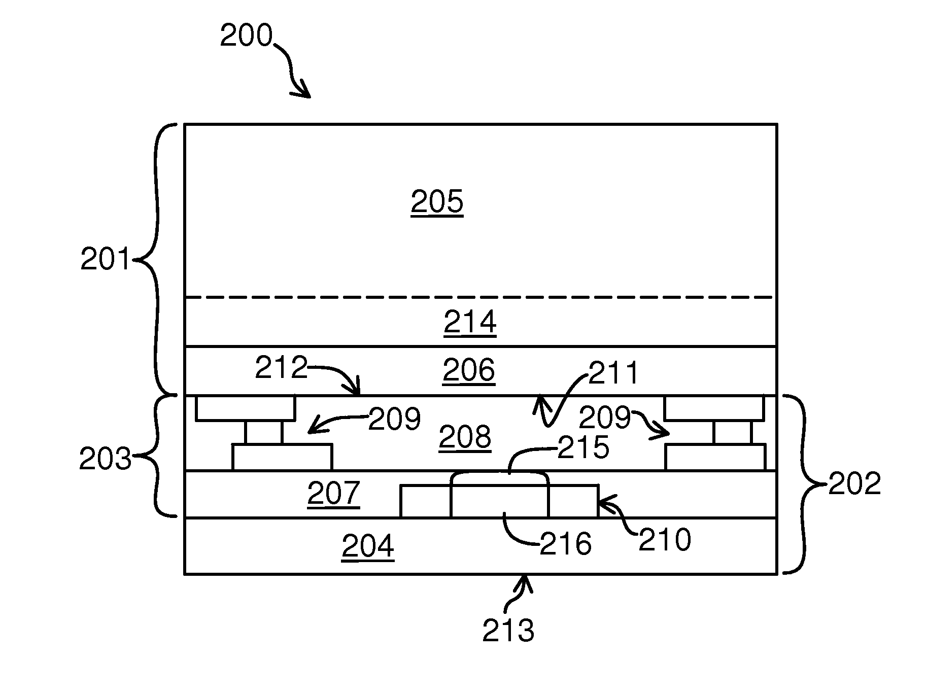
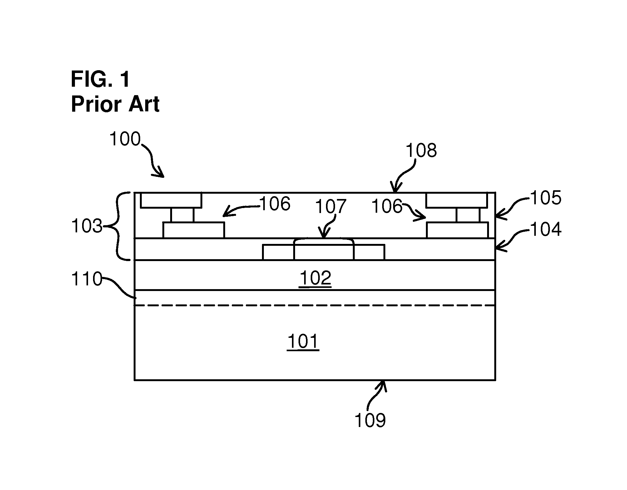
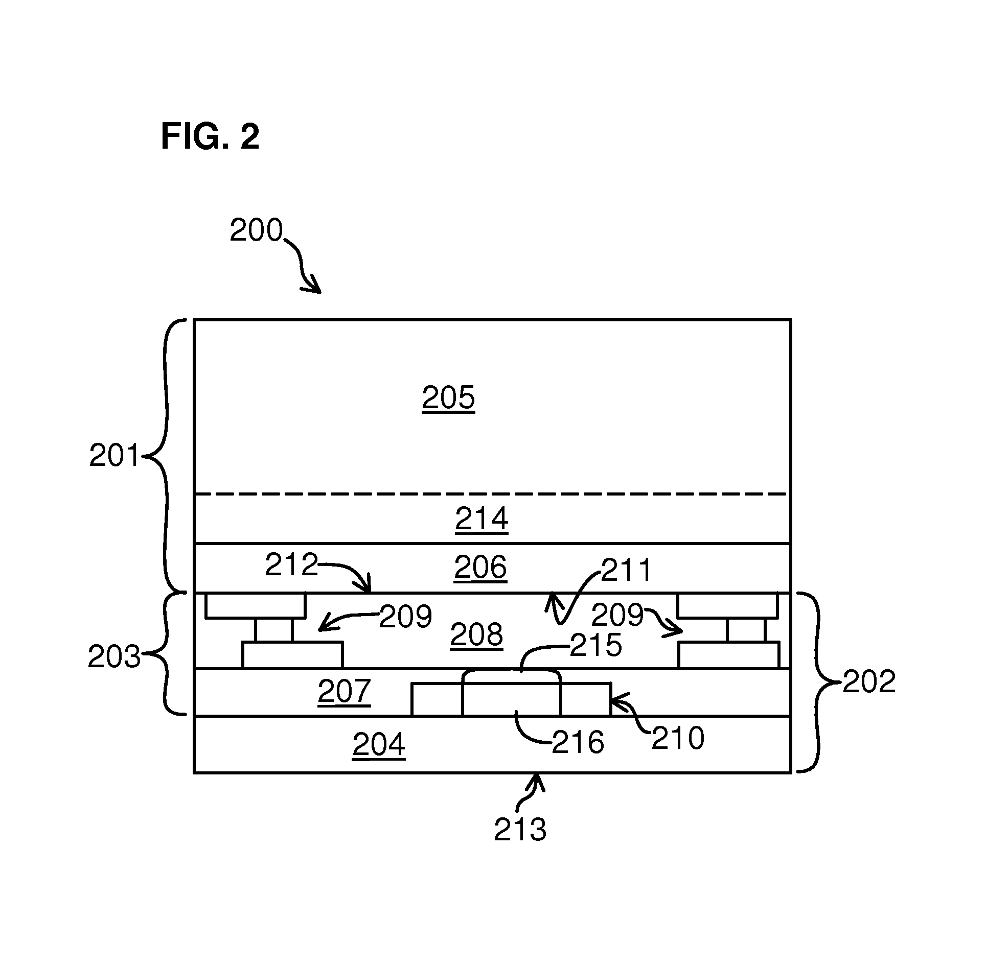
[0028]Reference now will be made in detail to example embodiments of the disclosed invention, one or more examples of which are illustrated in the accompanying drawings. Each example is provided by way of explanation of the present technology, not as a limitation of the present technology. In fact, it will be apparent to those skilled in the art that modifications and variations can be made in the present technology without departing from the spirit and scope thereof. For instance, features illustrated or described as part of one embodiment may be used with another embodiment to yield a still further embodiment. Thus, it is intended that the present subject matter covers all such modifications and variations within the scope of the appended claims and their equivalents.
[0029]Embodiments of the present invention generally inhibit parasitic surface conduction and enhance the RF performance of devices formed in one or more active layers of IC chips. Some embodiments of the present inve...
PUM
Property
Measurement
Unit
Semiconductor properties
aaaaa
aaaaa
Abstract
A semiconductor wafer is formed with a first device layer having active devices. A handle wafer having a trap rich layer is bonded to a top surface of the semiconductor wafer. A second device layer having a MEMS device or acoustic filter device is formed on a bottom surface of the semiconductor wafer. The second device layer is formed either by monolithic fabrication processes or layer-transfer processes.
Description
CROSS-REFERENCE TO RELATED APPLICATIONS[0001]This application is a continuation-in-part of U.S. patent application Ser. No. 14 / 043,764 filed Oct. 1, 2013, which is a continuation of U.S. patent application Ser. No. 13 / 762,257 filed Feb. 7, 2013, now U.S. Pat. No. 8,581,398, which is a continuation of U.S. patent application Ser. No. 13 / 652,240 filed Oct. 15, 2012, now U.S. Pat. No. 8,481,405, which is a continuation-in-part of U.S. patent application Ser. No. 13 / 313,231 filed Dec. 7, 2011, now U.S. Pat. No. 8,466,036, which claims priority to U.S. Provisional Patent Application No. 61 / 427,167 filed Dec. 24, 2010, under 35 U.S.C. §119(e), all of which are incorporated herein by reference in their entirety.BACKGROUND OF THE INVENTION[0002]Semiconductor-on-insulator (SOI) technology, which represents an advance over traditional bulk silicon processes, was first commercialized in the late 1990s. The defining characteristic of SOI technology is that the semiconductor region in which circ...
Claims
Application Information
Patent Timeline
Application Date:The date an application was filed.
Publication Date:The date a patent or application was officially published.
First Publication Date:The earliest publication date of a patent with the same application number.
Issue Date:Publication date of the patent grant document.
PCT Entry Date:The Entry date of PCT National Phase.
Estimated Expiry Date:The statutory expiry date of a patent right according to the Patent Law, and it is the longest term of protection that the patent right can achieve without the termination of the patent right due to other reasons(Term extension factor has been taken into account ).
Invalid Date:Actual expiry date is based on effective date or publication date of legal transaction data of invalid patent.