Localized fin width scaling using a hydrogen anneal

a hydrogen anneal and fin technology, applied in the direction of basic electric elements, electrical equipment, semiconductor devices, etc., can solve the problems of increasing short channel current leakage, increasing short channel effect, and presenting its own challenges in the reduction of fin width

Active Publication Date: 2014-12-04
RENESAS ELECTRONICS CORP +1
View PDF6 Cites 18 Cited by
  • Summary
  • Abstract
  • Description
  • Claims
  • Application Information

AI Technical Summary

Benefits of technology

[0007]A method for fabricating a transistor includes forming one or more semiconductor fins on a substrate; covering source and drain regions of the one or more semiconductor fins with a protective layer; annealing uncover

Problems solved by technology

As the gate length decreases, short channel current leakage increases.
Because new technologies are capable of forming progressively smaller transistors, these short channel effects become significant challenges in transistor design.
However, uniformly decreasing the size of fins presents its own challenges.
This increases the effective resistance of the thinner fin, which impacts

Method used


Image

  • Localized fin width scaling using a hydrogen anneal
  • Localized fin width scaling using a hydrogen anneal
  • Localized fin width scaling using a hydrogen anneal

Examples


Embodiment Construction

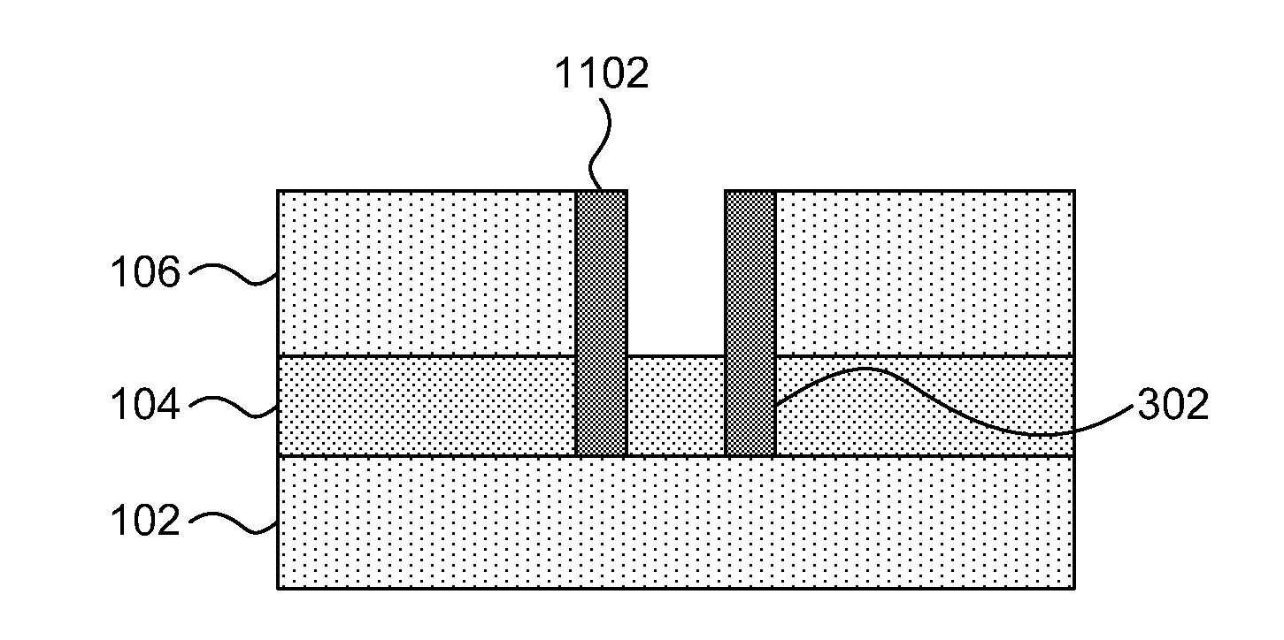
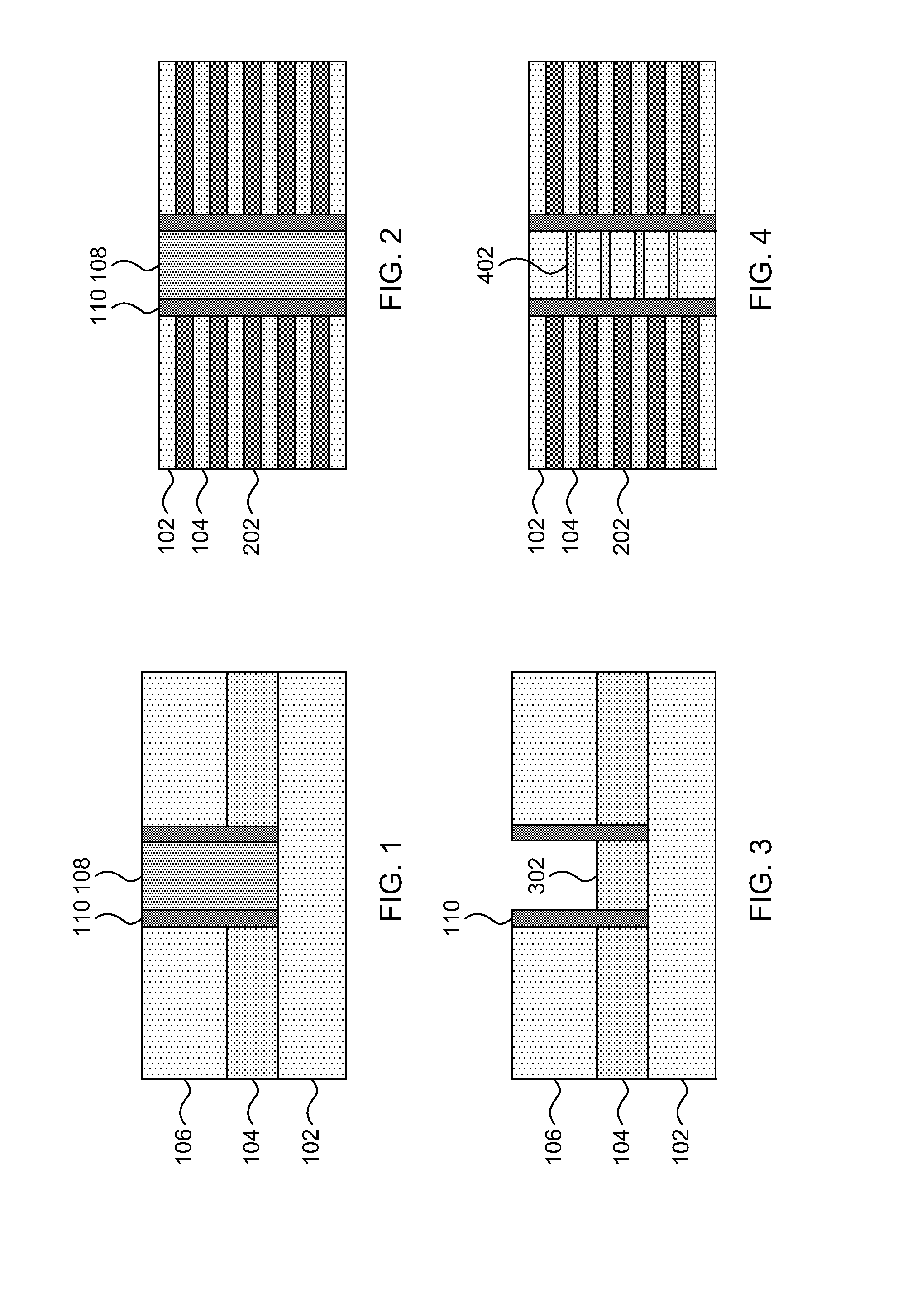
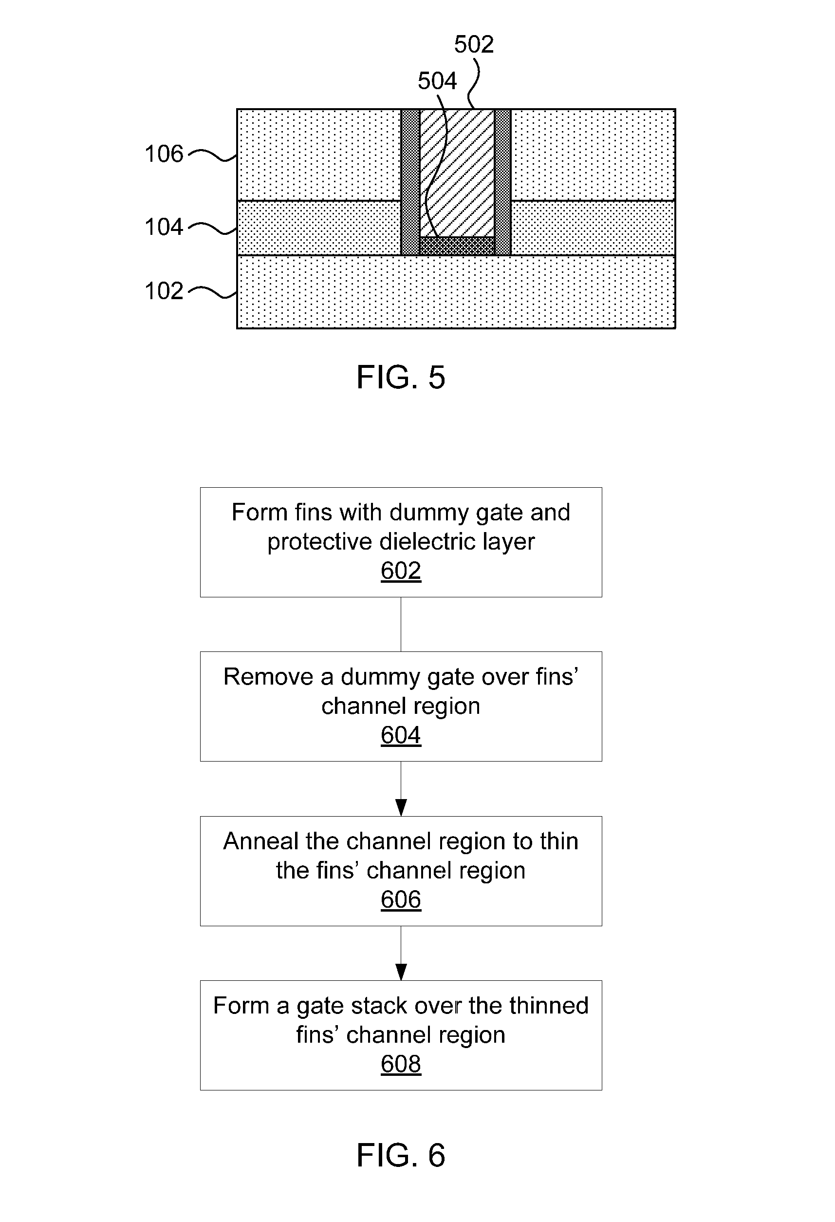
[0023]The present principles provide fin field effect transistors (FinFETs) that have fins with reduced width localized to the channel region. Short channel effects in transistors can be controlled if Wfingate, where Wfin is the width of the fin and Lgate is the length of the gate. Current crowding is a further concern, because reducing the fin width in the area of the source and drain region can cause a nonhomogeneous distribution of current density, which can lead to an increased effective resistance and shortened device lifetime.

[0024]To keep fin widths low and allow for further reduction in gate length, the present principles apply a hydrogen anneal that removes material only from the channel region of the fins, preserving the width of the fins in the source / drain region. In this way, leakage current in the transistor's off state is reduced without increasing the exterior resistance of the fins in the source and drain regions. The fins are epitaxially grown in the source / drain r...


PUM


Abstract

Transistors and methods for fabricating the same include forming one or more semiconductor fins on a substrate; covering source and drain regions of the one or more semiconductor fins with a protective layer; annealing uncovered channel portions of the one or more semiconductor fins in a gaseous environment to reduce fin width and round corners of the one or more semiconductor fins; and forming a dielectric layer and gate over the thinned fins.

Description

BACKGROUND[0001]1. Technical Field[0002]The present invention relates to transistor fabrication and, more particularly, to the fabrication of transistors with thinned channel fins.[0003]2. Description of the Related Art[0004]Limits on length of gates in fin field effect transistors (FinFETs) are imposed by fin width. As the gate length decreases, short channel current leakage increases. Because new technologies are capable of forming progressively smaller transistors, these short channel effects become significant challenges in transistor design. Forming transistors with thinner fins helps enhance gate control over the transistor channel, thereby reducing current leakage.[0005]However, uniformly decreasing the size of fins presents its own challenges. When the width of a fin is reduced, current crowding at the fin's exterior increases. This increases the effective resistance of the thinner fin, which impacts the drive current performance of the FinFET. This compromises the benefits ...

Claims


Application Information

Patent Timeline
IPC IPC(8): H01L29/66H01L29/78
CPCH01L29/785H01L29/66795H01L29/66818H01L29/7854H01L29/7856H01L29/41791H01L29/7831H01L29/42392H01L21/3247H01L29/0676H01L29/41733H01L29/42384H01L29/78696H01L21/30604H01L21/823425H01L21/823431H01L29/0673H01L29/1037
Inventor BASKER, VEERARAGHAVAN S.MOCHIZUKI, SHOGOYAMASHITA, TENKOYEH, CHUN-CHEN
Owner RENESAS ELECTRONICS CORP
Why Eureka
Try Eureka