Built in self test and method for RF transceiver systems

a transceiver and self-testing technology, applied in the field of rf (radio frequency) transceivers, can solve the problems of reducing the quality factor q of the tank circuit, increasing the error rate of center frequency, and reducing the dynamic range of the integrated circuit transceiver circuitry. , to achieve the effect of improving the dynamic range of the integrated circuit transceiver circuitry and reducing power consumption

Active Publication Date: 2014-12-04
TEXAS INSTR INC
View PDF4 Cites 25 Cited by
  • Summary
  • Abstract
  • Description
  • Claims
  • Application Information

AI Technical Summary

Benefits of technology

[0020]It is an object of the invention to provide a circuit and method which avoid increase in power consumption and reduction of dynamic range of a transceiver due to variation in the resonant frequency of conventional integrated circuit resonators or tank circuits.
[0021]It is another object of the invention to provide a circuit and method which avoid increase in power consumption and reduction of dynamic range of a transceiver due to variation in the resonant frequency of conventional integrated circuit resonators or tank circuits caused by variations in the quality factor Q of the resonators or tank circuits due to variation in integrated circuit process parameters and / or chip temperature.
[0022]It is another object of the invention to provide a circuit and method which improve dynamic range per unit current consumption in low power transceivers.

Problems solved by technology

Therefore, the center frequency errors are caused more by the capacitance variation.
Prior attempts to reduce variations in the resonant frequency of integrated circuit transceiver tank circuits usually have reduced the quality factor Q of the tank circuits.
A decrease in the Q factor of a tank circuit increases its current consumption and therefore degrades filtering at RF frequencies.
Furthermore, these problems become more severe in transceivers that have wide operating bandswidths.)
It should be appreciated that a receiver signal reduction of as little as 5 or 6 dB can be very undesirable or even catastrophic, especially for low-power designs in which a few hundred microamperes of current is very significant.
Unfortunately, there has been no practical way of achieving the above-mentioned shift of a tank circuit resonance frequency needed to correct an erroneous value of the resonance frequency caused by the integrated circuit manufacturing process variation and the chip temperature variation.

Method used


Image

  • Built in self test and method for RF transceiver systems
  • Built in self test and method for RF transceiver systems
  • Built in self test and method for RF transceiver systems

Examples


Embodiment Construction

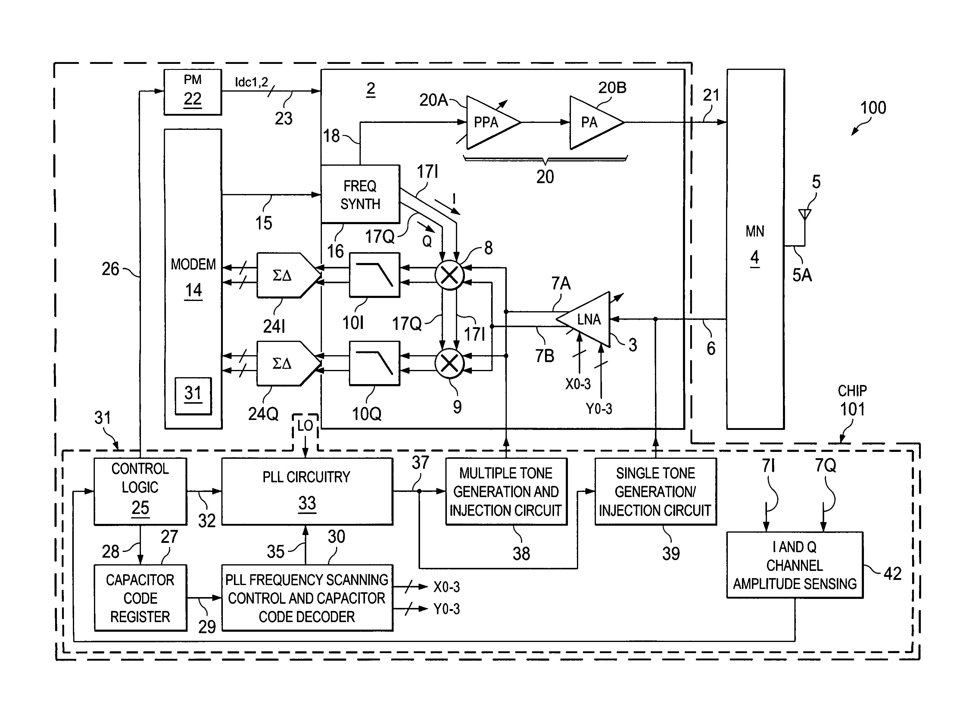
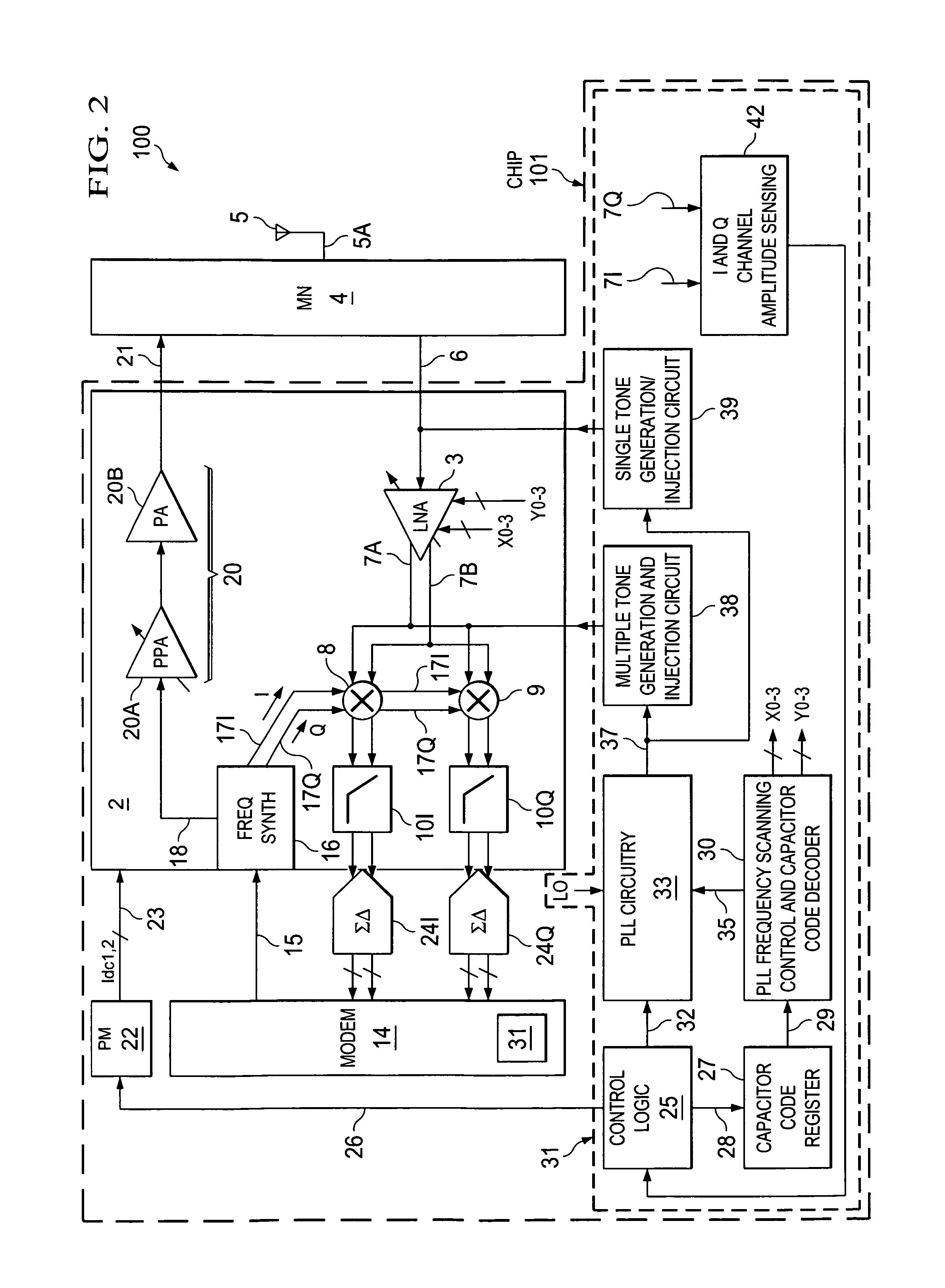
[0056]Built-in self-testing circuitry and methodology in an integrated circuit RF transceiver combine to automatically compensate for integrated circuit manufacturing process variations that are within worst-case (but not necessarily precisely known) values and also to compensate for chip temperature variations so as to maintain a high Q (qualify) factor of tank circuits in the transceiver, substantially reduce power consumption, and improve the dynamic range and tuning accuracy of the transceiver.

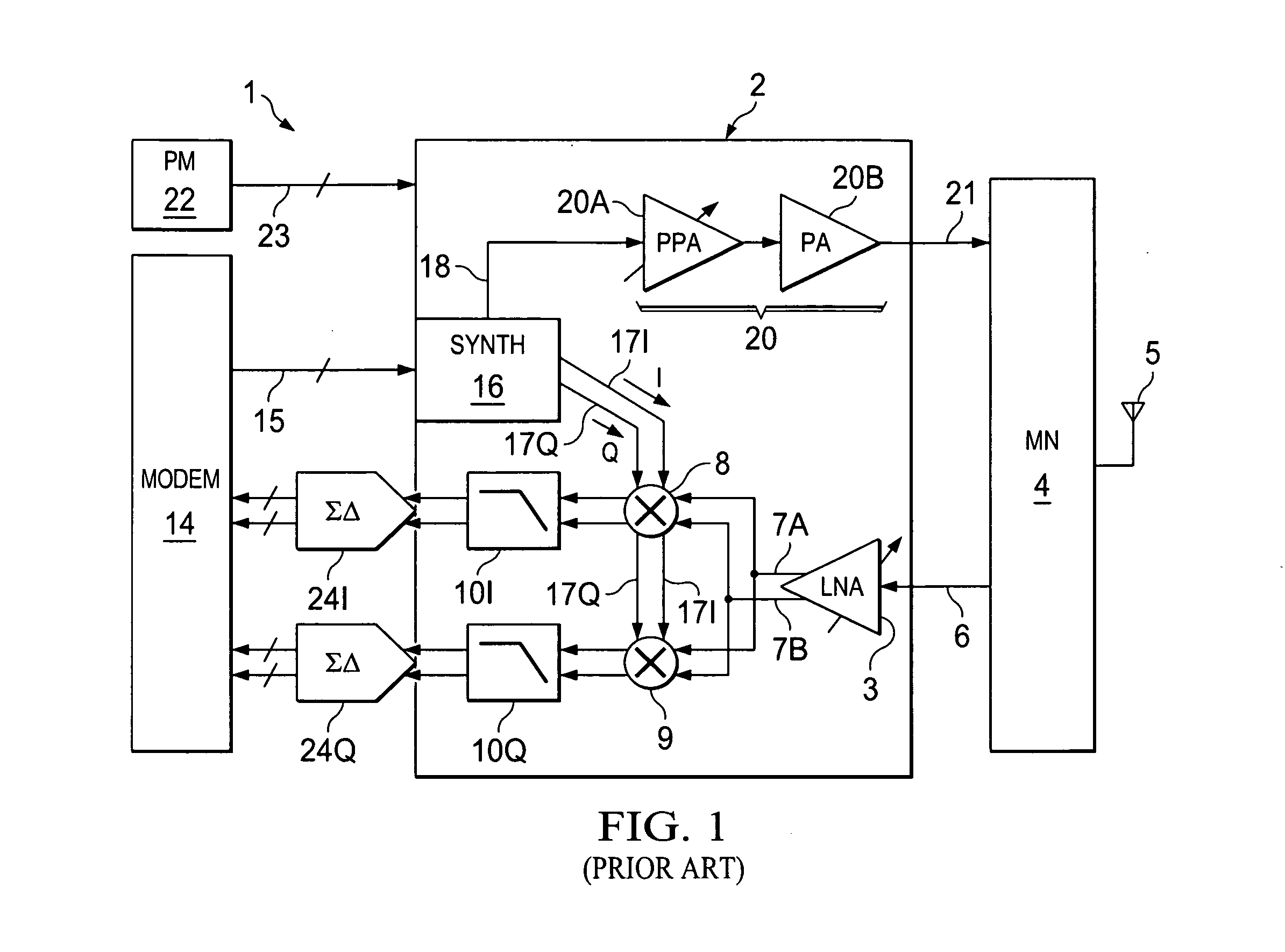
[0057]FIG. 2 illustrates a low-power, high dynamic range RF transceiver system 100 including an integrated circuit RF transceiver chip 101 and an external impedance matching network 4 which is connected to an external antenna 5. Transceiver-chip 101 in FIG. 2 includes a typical low-power RF front end circuit 2 coupled by impedance matching network 4 to antenna 5. A modem 14 is coupled to a “quadrature-phase channel” or “Q signal” channel of transceiver front end circuit 2 by means of a del...


PUM


Abstract

Integrated circuit transceiver circuitry (2) includes a first resonant circuit (3A) coupled to a narrowband interface (6,7A,7B,21) between a first amplifier (3,20) and an interfacing circuit (4,8,9,44), including a programmable first reactive element (C) and a second reactive element (L). Amplitude sensing circuitry (42) senses a maximum amplitude of an in-phase signal (I) or a quadrature-phase signal (Q). An on-chip first tone generation circuit (38,38A,38B,38C) generates tones for injection into the in-phase signal and the quadrature-phase signal and operates in response to frequency scanning circuitry (30) and the amplitude sensing circuitry to adjust the first reactive element (C) to calibrate the first resonant circuit to a desired resonant frequency by selectively coupling reactive sub-elements (1,2,4,8 . . . ×Cv) into the first reactive element (C).

Description

BACKGROUND OF THE INVENTION[0001]The present invention relates generally to RF (radio frequency) transceivers including circuitry for providing both reduced power consumption and increased dynamic range and accuracy, and more particularly to on-chip self test circuitry and methodology for reducing power consumption by automatically correcting for resonance frequency errors caused by integrated circuit process variation and the Q factor error caused by chip temperature variation.[0002]FIG. 1 illustrates an RF transceiver 1 including a typical low-power RF front end circuit 2 coupled by an impedance matching network 4 to an antenna 5. A modem 14 is coupled to a quadrature-phase signal channel Q of RF front end circuit 2 by means of a delta sigma ADC (analog to digital converter) 24Q and is coupled, in a in-phase signal channel 1 of RF front end circuit 2 by means of another delta sigma ADC 24I. A power management circuit 22 provides accurate DC voltages and DC currents required in RF ...

Claims


Application Information

Patent Timeline
Patent Type & Authority Applications(United States)
IPC IPC(8): H04B1/40H04B17/00
CPCH04B17/00H04B1/40H04W52/02H04W52/0261Y02D30/70
Inventor CHAKRABORTY, SUDIPTO
Owner TEXAS INSTR INC
Why Eureka
Try Eureka