
Multispectral sensor

a multi-spectral sensor and sensor technology, applied in the field of multi-spectral sensors, can solve problems such as registration errors

Active Publication Date: 2015-01-01
SOFTKINETIC SENSORS
View PDF27 Cites 111 Cited by
  • Summary
  • Abstract
  • Description
  • Claims
  • Application Information

AI Technical Summary

Benefits of technology

The present invention provides a sensor that can capture both color and depth images simultaneously using a single sensor. It also takes into account the distance-dependent factor, such as the reflectance of non-visible light, to create a more accurate and complete color / depth image. The sensor maximizes the optically active part of the pixel and avoids spatial aliazing errors without the need for interpolation. The technical effects of this invention are improved accuracy, efficiency, and a more complete capture of color and depth information in a single sensor.

Problems solved by technology

The so called image registration process is because the 2 imaging systems do not include necessarily lens having the same optical properties and because they may also not include the same resolution, and because they also are not necessarily well aligned.
Additionally, the RGBZ image is created by interpolating the Z pixels on the RGB pixels which is prone to registration errors.

Method used


Image

  • Multispectral sensor
  • Multispectral sensor
  • Multispectral sensor

Examples


first embodiment

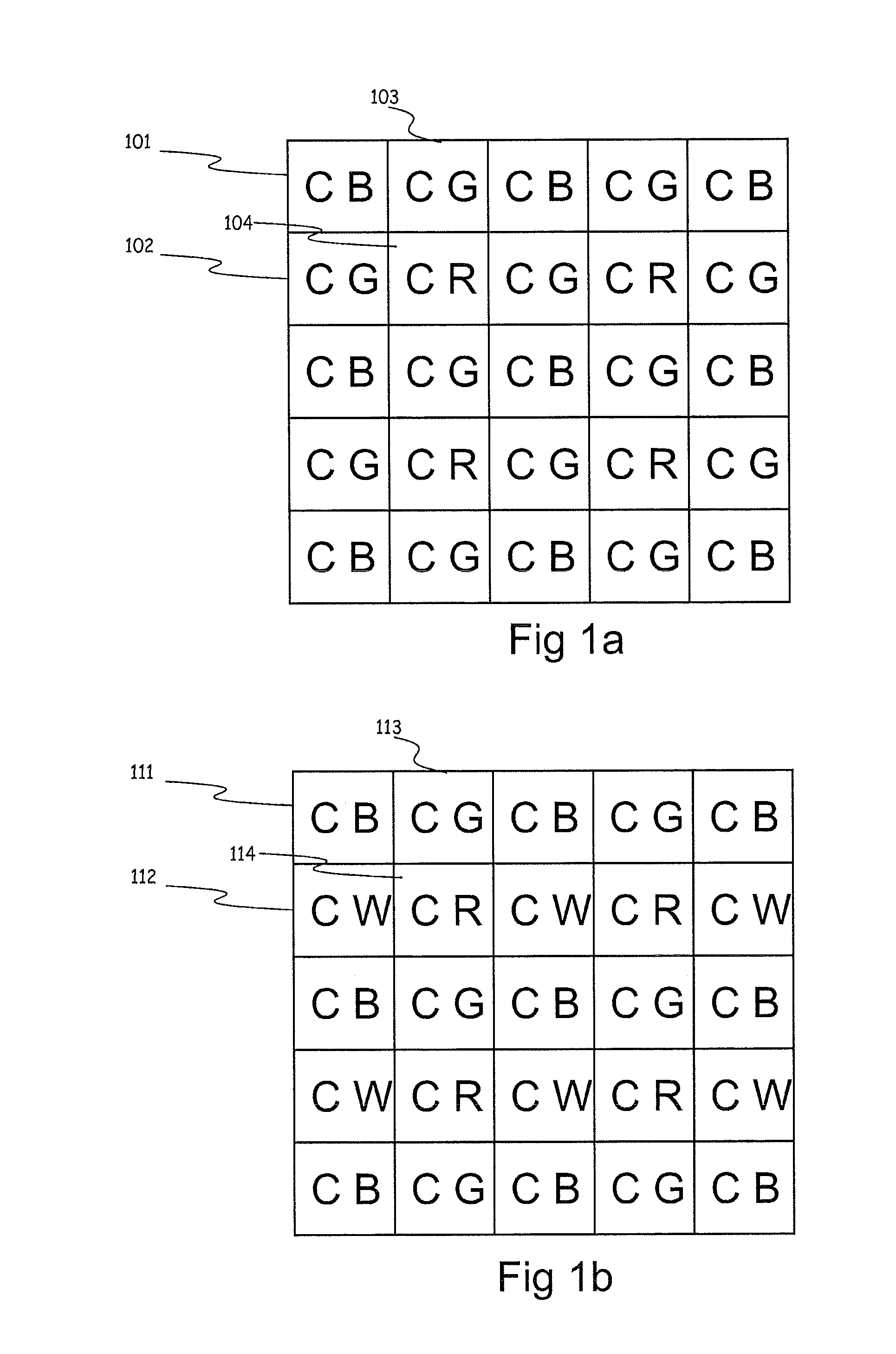
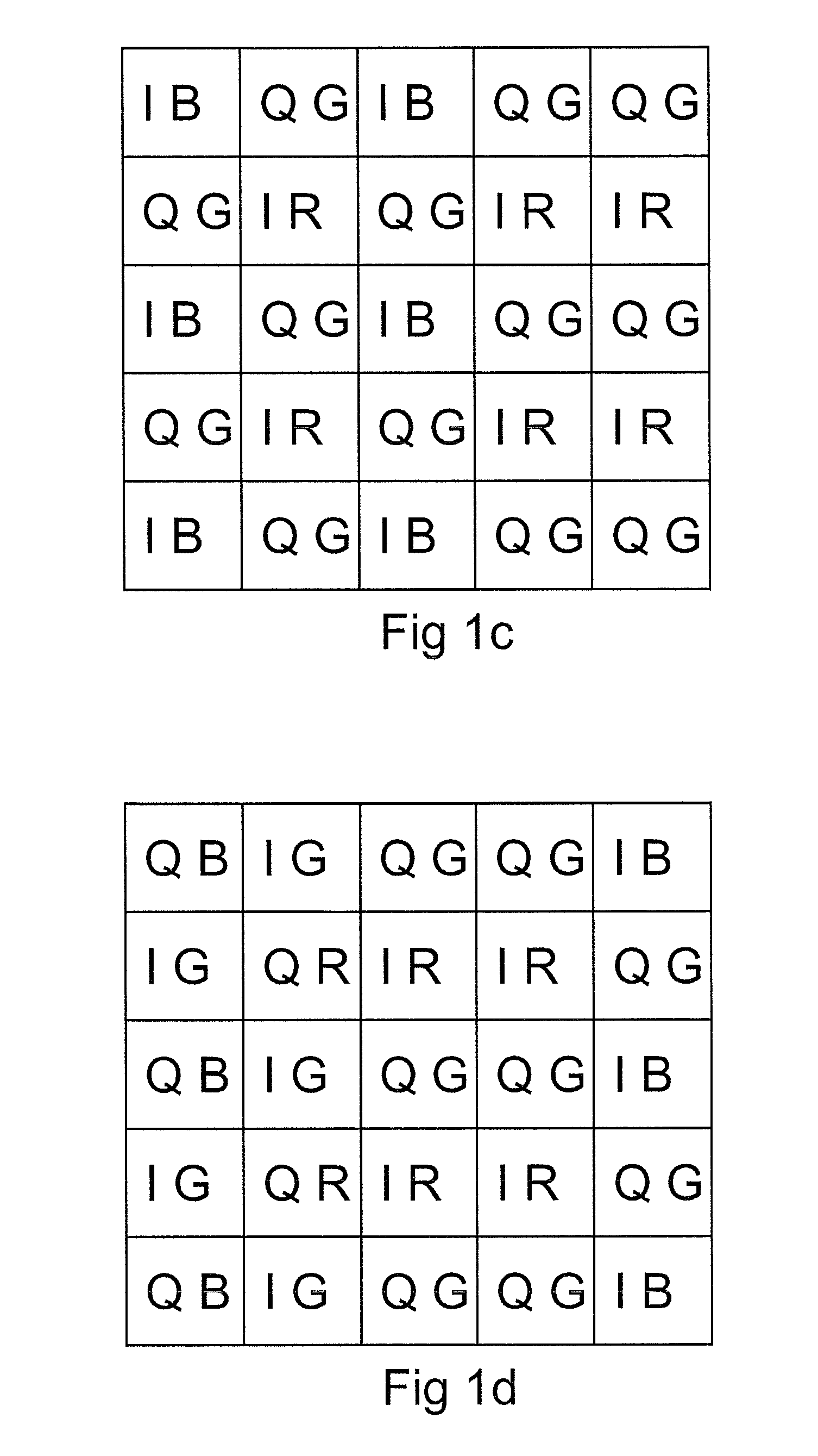
[0102]FIG. 1a shows the invention. The figure illustrates a pattern of pixels whereby individual pixels 101, 102, 103, 104 are capable of acquiring a non visible light, e.g. IR component which is at least 1 a correlation component (Ci) to reconstruct depth (Z) and at acquiring at least 1 color component. The non visible light, e.g. IR component can also provide a distance dependent factor such as a reflectance value of reflected non visible light, e.g. IR light from the object being viewed. Other distance dependent factors can be a speckle pattern, or a pattern that is actively projected onto the object. The distance dependent factor can be used to generate a confidence level. The color component can be for example R(ed), G(reen), B(lue), W(hite), etc. The color-pattern can be implemented according to state-of-the art patterns such as Bayer, RGBW, etc. Each pixel can be used to reconstruct depth and color offering the advantage of near-perfect registration. Pixels in an array do not...

second embodiment

[0103]FIG. 1b shows the inventions where pixels are capable of acquiring at least 1 correlation component to reconstruct depth and at least 1 color component R(ed), G(reen), B(lue) or W(hite).

[0104]A number of methods can be listed to reconstruct depth using spatially distributed, temporally distributed or spatially and temporally distributed correlation components. A pixel depth (Z) can be obtained using a single pixel and a single acquisition. Each pixel thus measures in a single optical acquisition (or exposure) all correlation components needed for a depth reconstruction.

[0105]Or the pixel depth (Z) can be obtained using 2 or more pixels and a single acquisition, each pixel measuring a correlation component necessary for the depth reconstruction. Each pixel thus measures at least 1 correlation component and may interpolates the missing correlation components using neighboring pixels. Methods for checking the consistency of the correlation components can be used to avoid combinin...

third embodiment

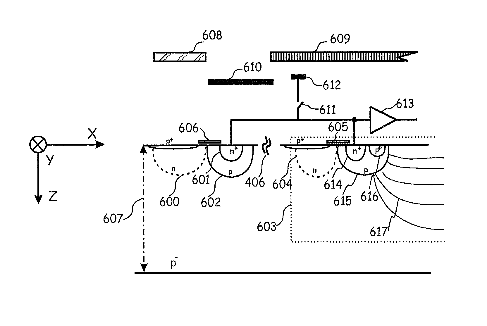
[0110]FIG. 3 shows the invention.

[0111]In the described embodiments of the present invention a CAPD is chosen as demodulation pixel, but the implementation can be independent of the demodulating device.

[0112]In FIG. 3 a Current-assisted photonic demodulator is shown whereby an electric field 307 is induced in a substrate 308 by a majority carrier current flowing between substrate terminals 301 and 302 or, in other words, first and second contact elements 301 and 302 (or vice versa). The substrate between the terminals 301 and 302 forms a first area sensitive to electromagnetic radiation, i.e. incident electromagnetic radiation, such as light for example, generates carriers in the substrate. The wavelength of the radiation that is effective in generation, e.g. speed of operation, depends upon the material of the substrate used as well as other factors such as temperature. Alongside substrate contacts or contact elements 301, 302 is a first and second detector 303, 304 respectively in...


PUM


Abstract

The present invention relates to a color and non-visible light e.g. IR sensor, namely a multispectral sensor which can be used in a camera such as a TOF camera for depth measurement, reflectance measurement and color measurement, and for generation of 3D image data or 3D images as well as the camera itself and methods of operating the same.

Description

[0001]The present invention relates to a color and non-visible light e.g. IR sensor, namely a multispectral sensor which can be used in a camera such as a TOF camera for depth measurement, reflectance measurement and color measurement, and for generation of 3D image data or 3D images as well as the camera itself and methods of operating the same.TECHNICAL BACKGROUND[0002]A camera has a plane receiving surface and based on this surface a co-ordinate system can be defined in which x, y is in the plane of that surface of the camera and z is an axis along the optical path of the camera. Time-of-Flight imaging systems measure the time difference or phase difference between pulsed light emitted from LED's or lasers, e.g. laser diodes, and the reflected pulses. In 3D Time-of-Flight imaging systems, a crucial functionality is to provide not only z data (z being the measured depth map) of the scene in the field of view of the camera, but also IR illumination and color data of the viewed scen...

Claims


Application Information

Patent Timeline
Patent Type & Authority Applications(United States)
IPC IPC(8): H01L27/146G01S7/4914G01S17/894
CPCH01L27/14645H01L27/14612H01L27/14621G01J2003/2826G01S7/4914G01S17/89H01L27/14623H01L27/14643G01S17/894H04N25/705
Inventor VAN DER TEMPEL, WARDVAN NIEUWENHOVE, DANIELKUIJK, MAARTEN
Owner SOFTKINETIC SENSORS
Learn More