Semiconductor device

a technology of mikro-conductor and reverse withstand voltage, which is applied in the direction of mikro-conductor devices, basic electric elements, electrical appliances, etc., can solve the problems of not easy to the reverse withstand voltage vr is lowered, and the reverse withstand voltage vr is not easy to lower. vf or shorten the reverse recovery time trr, etc., to achieve the effect of lowering the leak current ir

Active Publication Date: 2015-01-01
SHINDENGEN ELECTRIC MFG CO LTD
View PDF1 Cites 5 Cited by
  • Summary
  • Abstract
  • Description
  • Claims
  • Application Information

AI Technical Summary

Benefits of technology

[0020]According to the semiconductor device of the present invention, the semiconductor device has the structure where the barrier metal layer is formed on the surface of the second semiconductor layer and the surface of the high concentration diffusion region (that is, the JBS structure). Accordingly, at the time of applying a reverse bias, the whole region of a surface of the second semiconductor layer is pinched off due to a depletion layer extending toward a second semiconductor layer side from a boundary surface between the second semiconductor layer and the high concentration diffusion region and hence, a reverse withstand voltage VR can be increased and, at the same time, a leak current IR can be lowered.
[0021]According to the semiconductor device of the present invention, heavy metal is diffused in the semiconductor base body such that the concentration of heavy metal becomes maximum in a surface of the second semiconductor layer and hence, a depletion layer simulatively extends in the vicinity of the surface of the second semiconductor layer in the same manner as the case where the concentration of an impurity of a first conductive type is lowered. Accordingly, in the semiconductor device of the present invention, the whole region of the surface of the second semiconductor layer can be easily pinched off at the time of applying a reverse bias (see FIG. 1C described later) and hence, it is possible to lower a forward drop voltage VF or to shorten a reverse recovery time trr compared to the con...

Problems solved by technology

Accordingly, there exists a drawback that in an actual operation, it is not easy to lower a forward drop voltage VF or to shorten a reverse recovery time trr while maintaining a high reverse withstand voltag...

Method used


Image

  • Semiconductor device
  • Semiconductor device
  • Semiconductor device

Examples


embodiment 1

A. Semiconductor Device 100 According to Embodiment 1

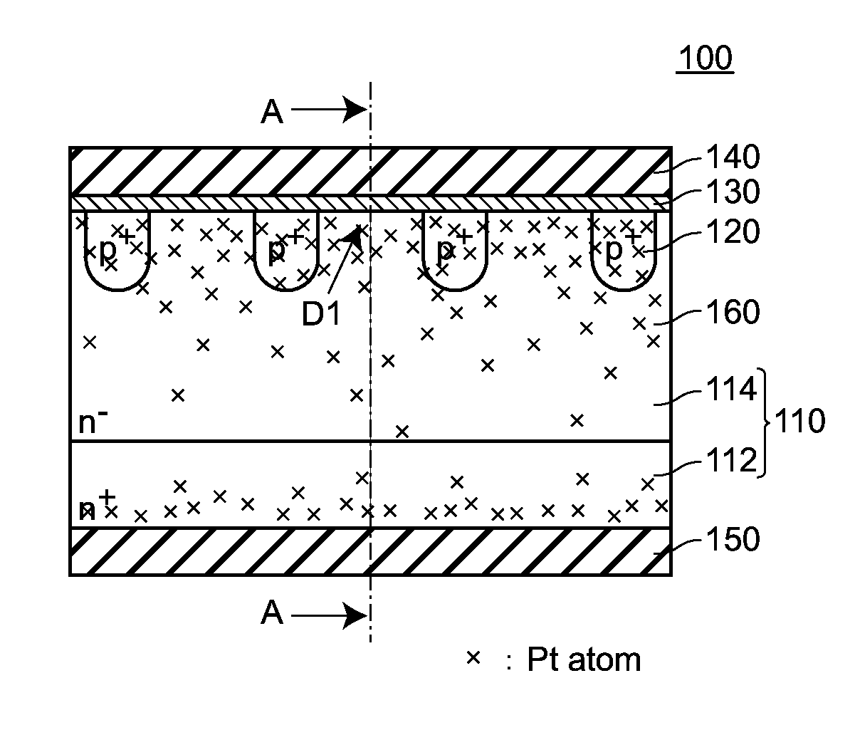
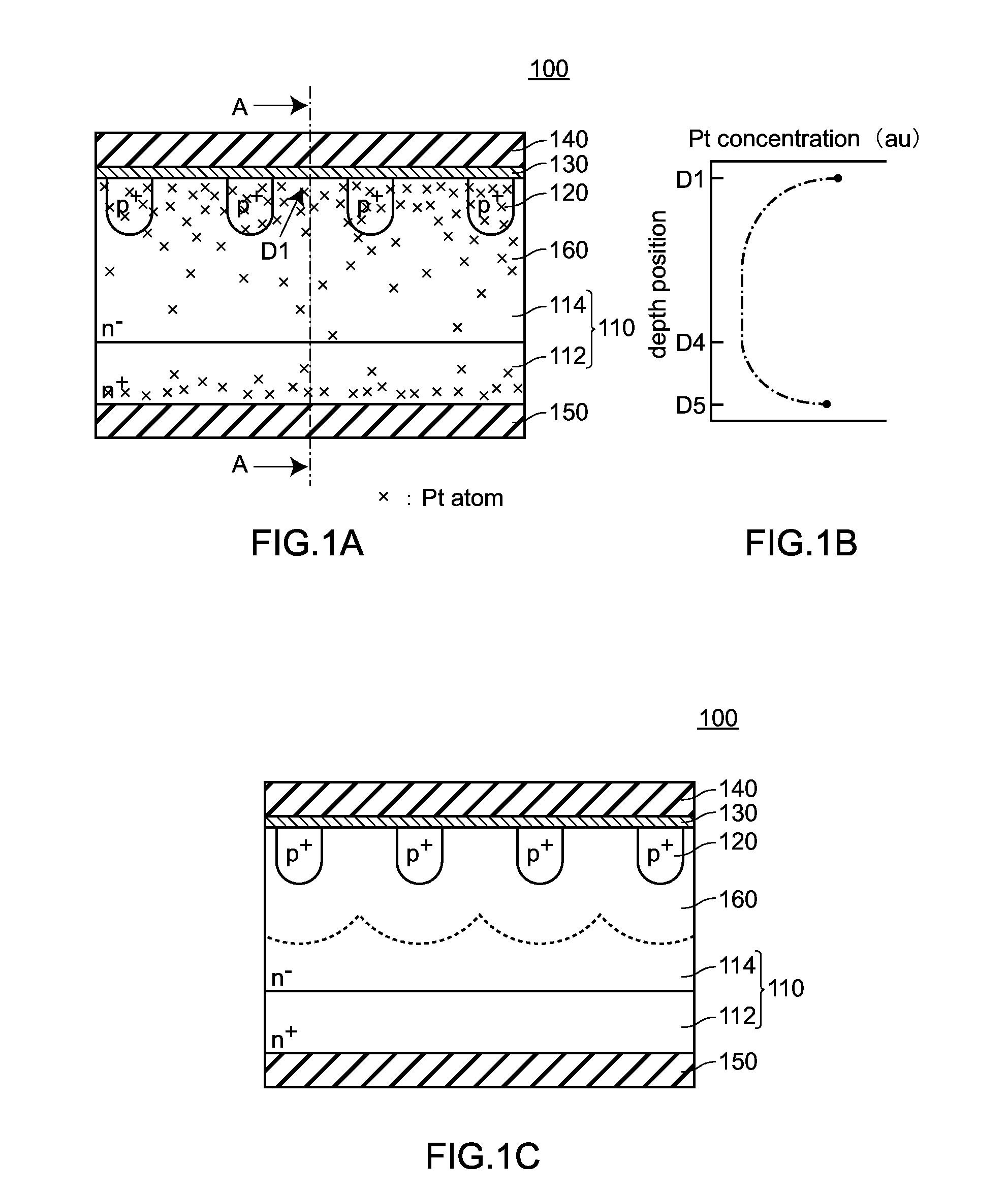
[0046]FIG. 1A to FIG. 1C are views for explaining a semiconductor device 100 according to the embodiment 1. FIG. 1A is a cross-sectional view of the semiconductor device 100, FIG. 1B is a graph showing the concentration distribution of heavy metal (platinum) in a semiconductor base body 110, and FIG. 1C is a view showing a state where a depletion layer 160 extends when a reverse bias is applied to the semiconductor device 100.

[0047]As shown in FIG. 1, the semiconductor device 100 according to the embodiment 1 includes: a semiconductor base body 110 having the structure where an n+-type semiconductor layer (a first semiconductor layer of a first conductive type) 112 and an n−-type semiconductor layer (a second semiconductor layer of a first conductive type) 114 containing an impurity of an n-type (an impurity of a first conductive type) at a concentration lower than a concentration of the impurity of the first conductive type conta...

modification 1

[Modification 1]

[0081]FIG. 5A to FIG. 5D are views for explaining a method of manufacturing a semiconductor device according to a modification 1 of the embodiment 1. FIG. 5A to FIG. 5D are views showing respective steps of the method. In the method of manufacturing a semiconductor device according to the modification 1 of the embodiment 1, steps following a heavy metal diffusion source layer forming step (see FIG. 3D to FIG. 4D) are substantially equal to the corresponding steps in the method of manufacturing a semiconductor device according to the embodiment 1 and hence, the illustrations of the steps corresponding to the steps shown in FIG. 3D to FIG. 4D are omitted.

[0082]Although the method of manufacturing a semiconductor device according to the modification 1 of the embodiment 1 basically includes the substantially same steps as the method of manufacturing a semiconductor device according to the embodiment 1, the modification 1 differs from the embodiment 1 with respect to a ty...

modification 2

[Modification 2]

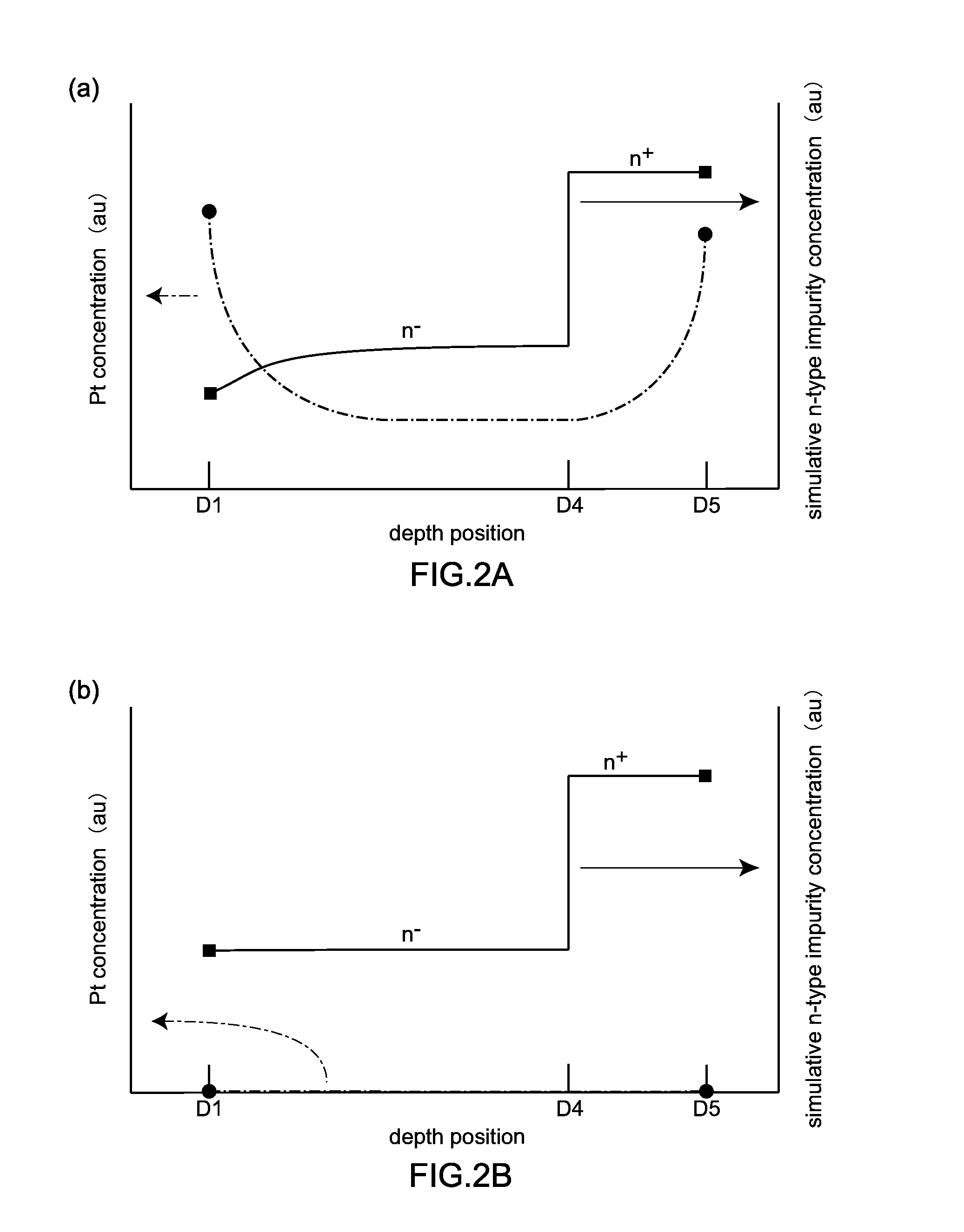
[0085]FIG. 6A and FIG. 6B are views for explaining a method of manufacturing a semiconductor device according to a modification 2 of the embodiment 1. FIG. 6A and FIG. 6B are views showing respective steps of the method. FIG. 7A and FIG. 7B are views for explaining a semiconductor device 100b according to the modification 2 of the embodiment 1. FIG. 7A is a cross-sectional view of the semiconductor device 100b, and FIG. 7B is a graph showing the concentration distribution of heavy metal (platinum) in the semiconductor base body 110. In the method of manufacturing a semiconductor device according to the modification 2 of the embodiment 1, steps up to a heavy metal diffusion source layer forming step (see FIG. 3A to FIG. 3C) and steps following a barrier metal layer forming step (see FIG. 4C to FIG. 4D) are substantially equal to the corresponding steps in the method of manufacturing a semiconductor device according to the embodiment 1 and hence, the illustrations of t...


PUM


Abstract

A semiconductor device includes a semiconductor base body having an n+-type semiconductor layer and an n-type semiconductor layer p+-type diffusion regions selectively formed on a surface of the n-type semiconductor layer, and a barrier metal layer formed on a surface of the n-type semiconductor layer and surfaces of p+-type diffusion regions. A Schottky junction is between the barrier metal layer and the n-type semiconductor layer. An ohmic junction is between the barrier metal layer and the p+-type diffusion regions. Platinum is diffused into the semiconductor base body such that a concentration of platinum becomes maximum in a surface of the n-type semiconductor layer.

Description

RELATED APPLICATIONS[0001]The present application is a National Phase of International Application Number PCT / JP2012 / 067018, filed Jul. 3, 2012.TECHNICAL FIELD[0002]The present invention relates to a semiconductor device.BACKGROUND ART[0003]Conventionally, there has been known a semiconductor device which is referred to as the JBS structure (for example, see Patent literature 1). FIG. 18A and FIG. 18B are views for explaining a conventional semiconductor device 900. FIG. 18A is a cross-sectional view schematically showing the conventional semiconductor device 900, and FIG. 18B is a view showing a state where a depletion layer 960 extends when a reverse bias is applied to the conventional semiconductor device 900. Since FIG. 18A and FIG. 18B are cross-sectional views which schematically show the conventional semiconductor device 900, the respective elements are drawn with suitable modification in these drawings. Accordingly, sizes of the respective elements, distances between the res...

Claims


Application Information

Patent Timeline
IPC IPC(8): H01L29/36H01L29/872
CPCH01L29/872H01L29/36H01L29/167H01L29/32H01L29/66143H01L21/221H01L21/2254H01L29/0619
Inventor MATSUZAKI, YOSHIFUMI
Owner SHINDENGEN ELECTRIC MFG CO LTD
Why Eureka
Try Eureka