Wiring board and method for manufacturing the same

a technology of wiring board and manufacturing method, which is applied in the direction of printed circuit manufacturing, printed circuit aspects, and dielectric characteristics, can solve the problems of difficulty in sufficiently ensuring the reliability of connections between the pads of the build-up wiring board and, for example, the electrodes of the semiconductor chip, and achieve the effect of enhancing the reliability of connections

Active Publication Date: 2015-01-15
SHINKO ELECTRIC IND CO LTD
View PDF6 Cites 16 Cited by
  • Summary
  • Abstract
  • Description
  • Claims
  • Application Information

AI Technical Summary

Benefits of technology

[0010]The disclosed technique makes it possible to provide a wiring board, etc

Problems solved by technology

As a result, the surfaces of the pads are lowered in solder wettability, which may lead to that it is difficult to sufficiently ensure

Method used


Image

  • Wiring board and method for manufacturing the same
  • Wiring board and method for manufacturing the same
  • Wiring board and method for manufacturing the same

Examples


Embodiment Construction

[0019]Exemplary embodiments of the invention will be hereinafter described with reference to the accompanying drawings. In the drawings, the same constituent elements will be given the same reference symbol and may not be described redundantly.

Structure of Wiring Board According to One Exemplary Embodiment

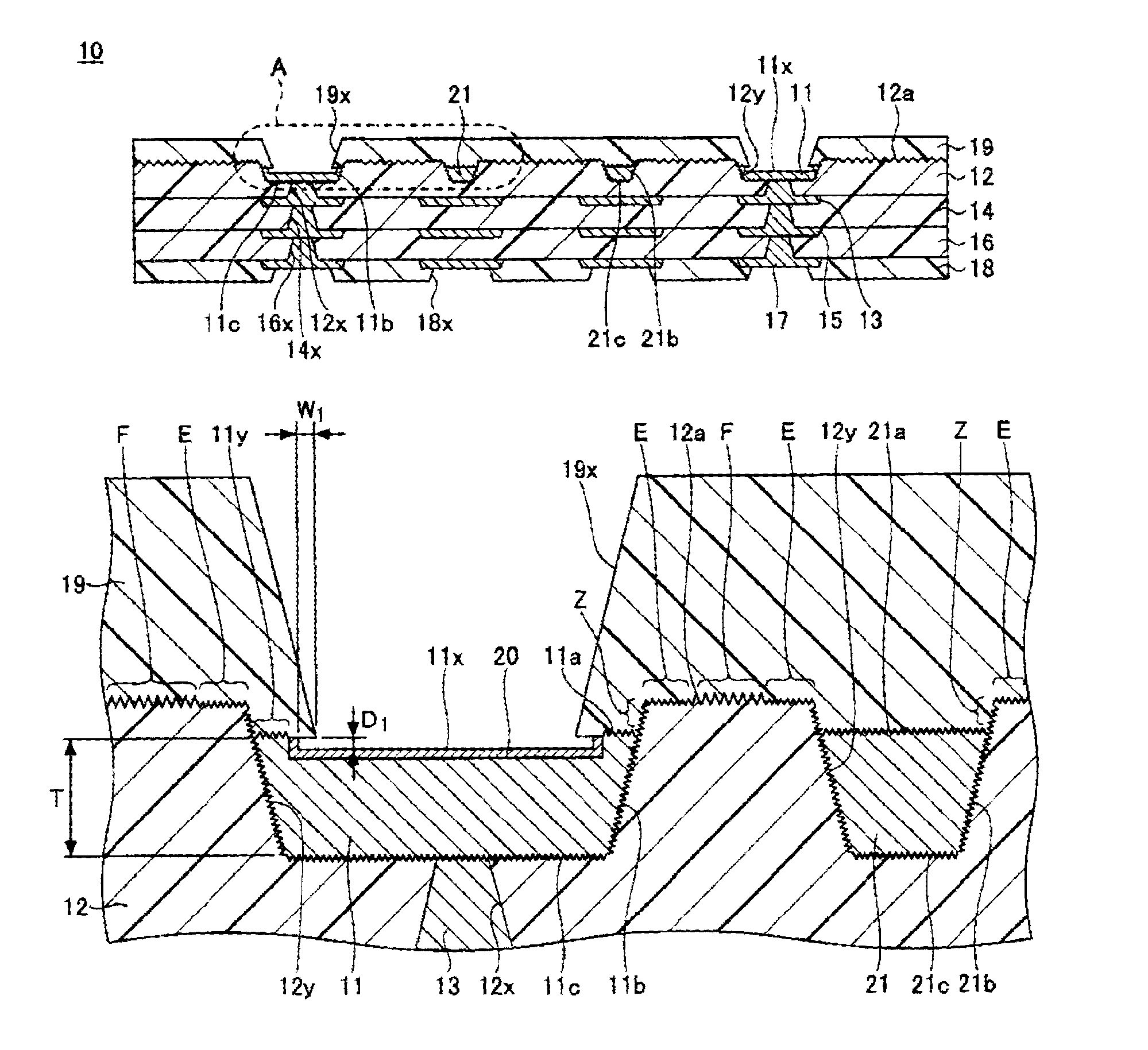
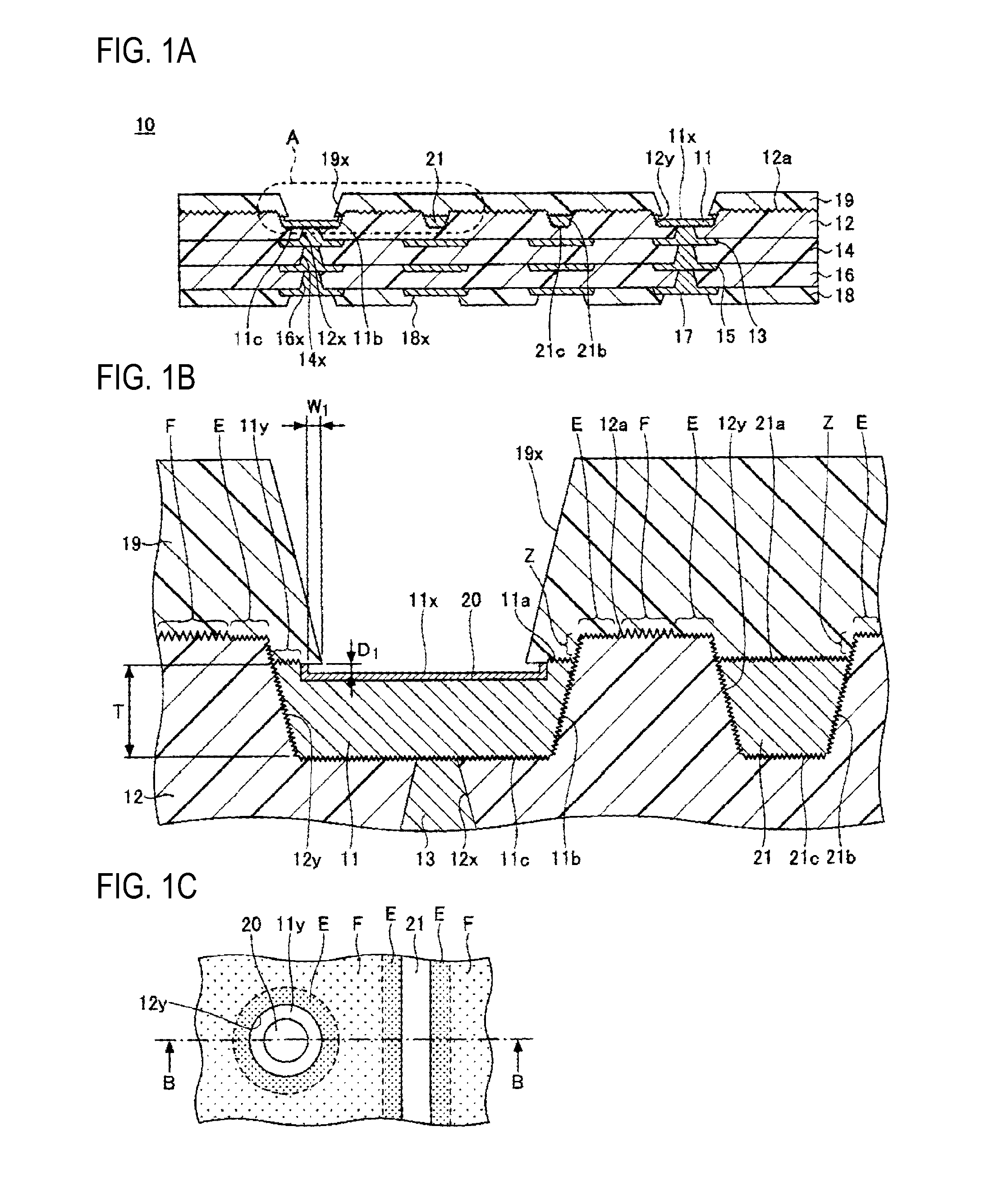
[0020]First, a structure of a wiring board according to a first exemplary embodiment will be described. FIG. 1A is a section view of the wiring board according to the exemplary embodiment. FIG. 1B is an enlarged section view, taken along a line B-B in FIG. 1C, of a part A of FIG. 1A. FIG. 1C is an enlarged plan view of the part A of FIG. 1A. Surface-treated layers 20 are omitted in FIG. 1A, and a solder resist layer 19 is omitted in FIG. 1C.

[0021]As shown in FIGS. 1A to 1C, the wiring board 10 according to the exemplary embodiment has pads 11, an insulating layer 12, a wiring layer 13, an insulating layer 14, a wiring layer 15, an insulating layer 16, a wiring layer 17, solder resi...


PUM


Abstract

A wiring substrate includes an insulating layer, a pad, and a solder resist layer. The insulating layer has a first surface formed with a first recess portion. The pad is embedded in the first recess portion. The pad includes a second surface and a third surface. The third surface that is located at a lower position than the first surface so as to expose an inner wall surface of the first recess portion. The pad is formed with a second recess portion in a center portion of the third surface. The solder resist layer is provided on the first surface. An adjacent portion of the first surface to a peripheral portion of the first recess portion is smaller in roughness than a region of the first surface peripheral to the adjacent portion of the first surface.

Description

CROSS-REFERENCE TO RELATED APPLICATION(S)[0001]This application claims priority from Japanese Patent Application No. 2013-145914, filed on Jun. 11, 2013, the entire contents of which are herein incorporated by reference.BACKGROUND[0002]1. Field[0003]Exemplary embodiments of the invention relate to a wiring board and a method for manufacturing the wiring board.[0004]2. Related Art[0005]What is called build-up wiring boards are known in which wiring layers and insulating layers are stacked alternately and the wiring layers are connected to each other through via holes which penetrate through the insulating layers. For example, such build-up wiring boards are manufactured by stacking wiring layers and insulating layers on a support body and then removing the support body.[0006]In a manufacturing process of a build-up wiring board, a surface of a support body may be roughened. In this case, when the support body is removed, the roughened surface of the support body is transferred to an ...

Claims


Application Information

Patent Timeline
IPC IPC(8): H05K1/11H05K1/03
CPCH05K2201/09381H05K2201/0104H05K2201/09472H05K1/0373H05K2201/0206H05K1/113H05K2201/09454H05K3/244H05K3/3452H05K3/383H05K3/4682H05K2201/09745H05K2201/2072H05K2203/0152H05K2203/0307H05K2203/0376H05K2203/0384H05K2203/1184H05K2203/308
Inventor KANEKO, KENTAROKOBAYASHI, KAZUHIROOMIYA, TOSHIMITSUKODANI, KOTAROMATSUMOTO, SHUNICHIROTANG, RUOFAN
Owner SHINKO ELECTRIC IND CO LTD
Why Eureka
Try Eureka