Organic light-emitting diode display and method of manufacturing the same

a light-emitting diode and display technology, applied in the direction of solid-state devices, semiconductor devices, thermoelectric devices, etc., can solve the problems of low voltage drive of oleds, short response time, wide viewing angle, etc., and achieve the effect of improving hole injection efficiency and improving hole injection efficiency

Inactive Publication Date: 2015-01-15
SAMSUNG DISPLAY CO LTD
View PDF5 Cites 9 Cited by
  • Summary
  • Abstract
  • Description
  • Claims
  • Application Information

AI Technical Summary

Benefits of technology

[0007]Exemplary embodiment of the invention provide an organic light-emitting diode display (“OLED”) having improved hole injection efficiency.
[0008]Exemplary embodiments of the invention also provide a method of manufacturing an OLED having improved hole injection efficiency.

Problems solved by technology

In particular, OLEDs can be driven at a low voltage and have a wide viewing angle and a short response time.

Method used


Image

  • Organic light-emitting diode display and method of manufacturing the same
  • Organic light-emitting diode display and method of manufacturing the same
  • Organic light-emitting diode display and method of manufacturing the same

Examples


Embodiment Construction

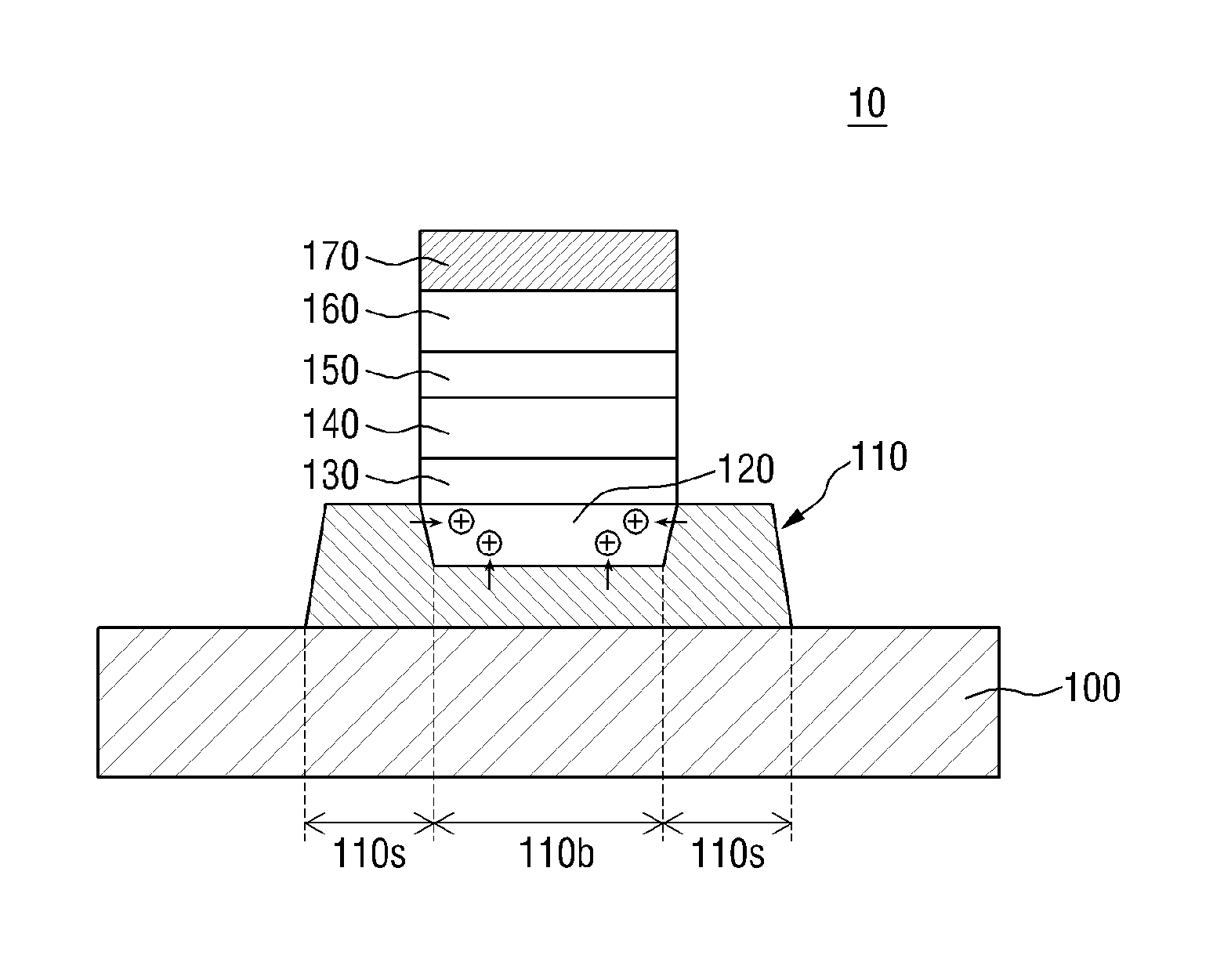
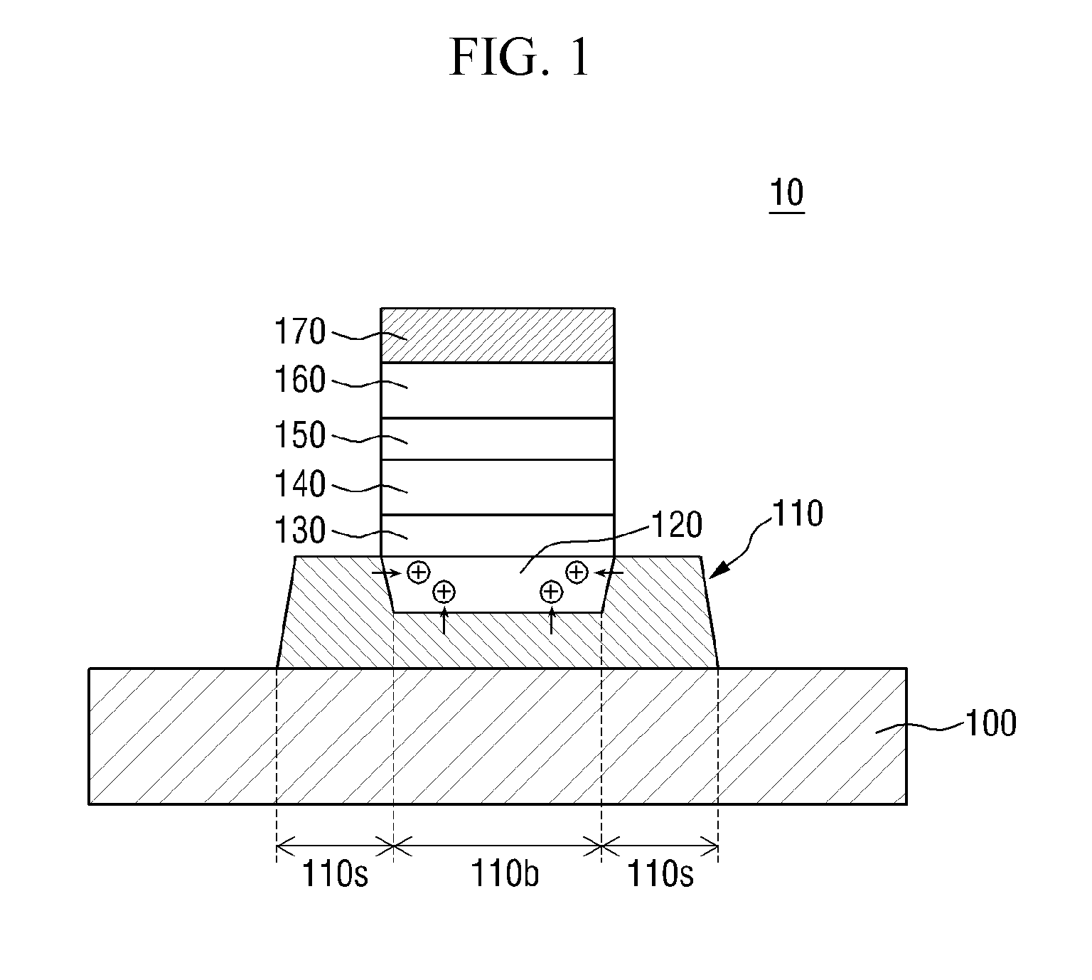
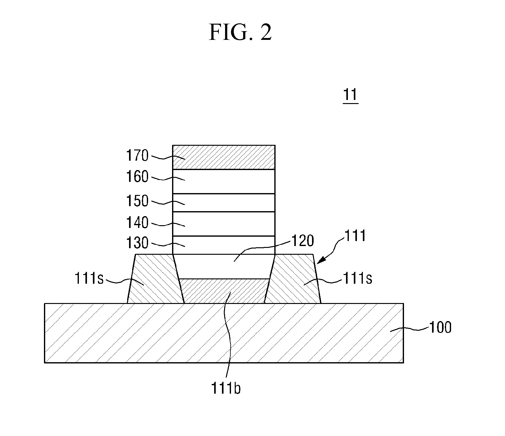
[0025]Light-emission efficiency increases as the injection efficiency of holes from the anode to the organic layer increases. Thus, a hole injection layer may be provided between the anode and the organic layer in order to increase the hole injection efficiency. However, when the hole injection layer is not placed at an exact position, sufficient hole injection efficiency cannot be ensured.

[0026]Advantages and features of the invention and methods of accomplishing the same may be understood more readily by reference to the following detailed description of exemplary embodiments and the accompanying drawings. The invention may, however, be embodied in many different forms and should not be construed as being limited to the exemplary embodiments set forth herein. Rather, these exemplary embodiments are provided so that this disclosure will be thorough and complete and will fully convey the concept of the invention to those skilled in the art, and the invention will only be defined by ...


PUM


Abstract

An organic light-emitting diode display includes a substrate, a first electrode which is disposed on the substrate, a trench defined in a top surface of the first electrode, and a hole injection layer which is disposed in the trench.

Description

[0001]This application claims priority to Korean Patent Application No. 10-2013-0082311 filed on Jul. 12, 2013, and all the benefits accruing therefrom under 35 U.S.C. §119, the disclosure of which is incorporated herein by reference in its entirety.BACKGROUND[0002]1. Field[0003]The invention relates to an organic light-emitting diode display (“OLED”) and a method of manufacturing the same.[0004]2. Description of the Related Art[0005]Demands for displays have been increased due to a development of information and communications technology and diverse needs of an information society. Cathode ray tubes (“CRTs”), which were once the most common type of displays, are being replaced by flat panel displays (“FPDs”) to meet demands for more compact and less power-consuming displays. Some of the most widely used FPDs include electroluminescent displays (“ELDs”), liquid crystal displays (“LCDs”), plasma display panels (“PDPs”), and organic light-emitting diode displays (“OLEDs”).[0006]In par...

Claims


Application Information

Patent Timeline
Patent Type & Authority Applications(United States)
IPC IPC(8): H01L51/50H01L51/56
CPCH01L51/56H01L51/5088H10K71/621H10K71/00H10K59/805H10K50/14H10K2102/351H10K50/805
Inventor KIM, SUK
Owner SAMSUNG DISPLAY CO LTD
Why Eureka
Try Eureka