Light emitting diode with electron blocking layer in resonant tunneling structure

A technology of light-emitting diodes and structural electronics, applied in circuits, electrical components, semiconductor devices, etc., can solve the problems of low carrier recombination efficiency and luminous efficiency of LED devices, achieve good electron blocking effect, simple growth mode, high-altitude Effect of Cave Injection Efficiency

Active Publication Date: 2017-09-22
SOUTHEAST UNIV
View PDF3 Cites 8 Cited by
  • Summary
  • Abstract
  • Description
  • Claims
  • Application Information

AI Technical Summary

Problems solved by technology

However, these electron blocking layers still cannot satisfactorily solve the biggest technical problem: the more obvious the blocking effect of the p-type electron blocking layer on electron leakage, the greater the drop in hole injection efficiency, thus leading to the carrier recombination of LED devices. Efficiency and luminous efficiency are still low

Method used


Image

  • Light emitting diode with electron blocking layer in resonant tunneling structure
  • Light emitting diode with electron blocking layer in resonant tunneling structure
  • Light emitting diode with electron blocking layer in resonant tunneling structure

Examples


Embodiment Construction

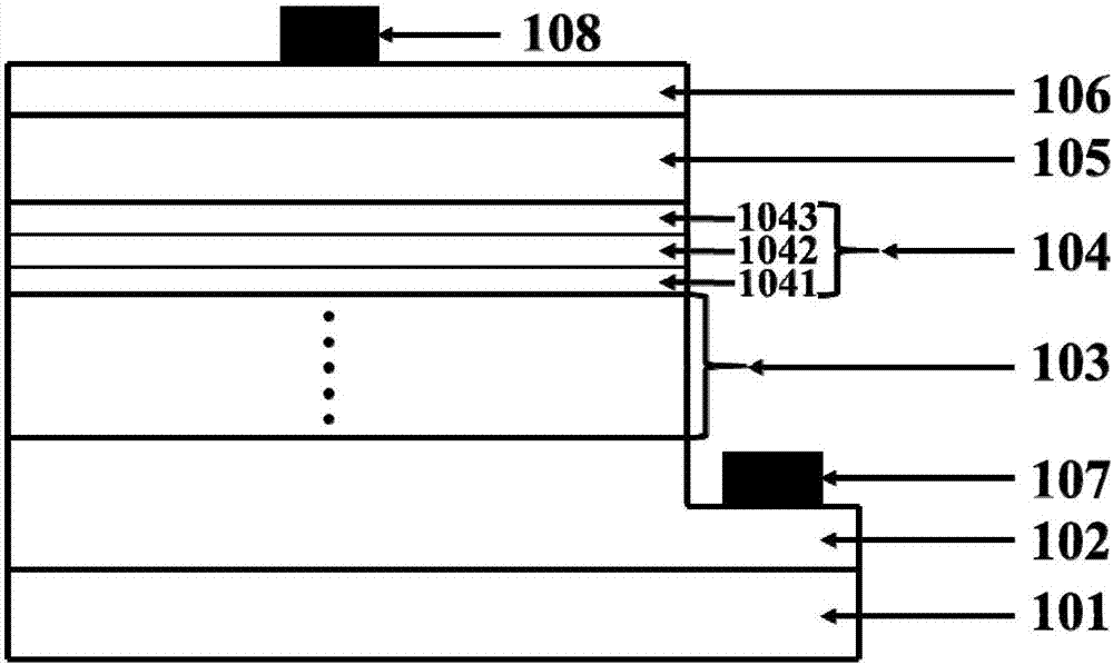
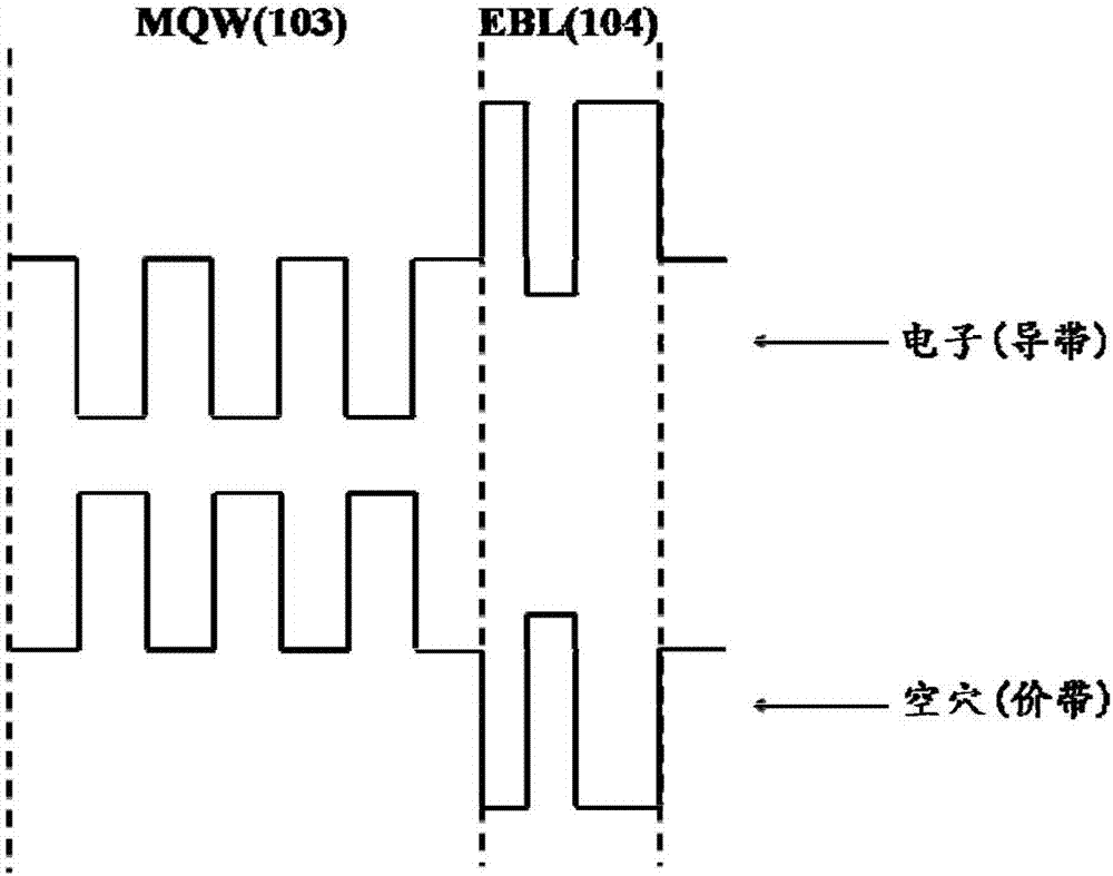
[0019] Such as figure 1 As shown, a light-emitting diode with a resonant tunneling structure electron blocking layer includes: an m-plane sapphire substrate 101, an n-type AlGaN layer 102, an AlGaN / AlN multi-quantum well layer 103, and a resonant tunneling structure arranged sequentially from bottom to top. Through structure electron blocking layer 104, p-type AlGaN layer 105, ITO ohmic contact layer 106, Ti metal layer set on the n-type AlGaN layer as n-type electrode 107 and Ni / Ag alloy set on the p-type AlGaN layer layer as a p-type electrode 108, wherein the electron blocking layer 104 is composed of a p-type doped AlGaN barrier layer 1041, a non-doped AlGaN potential well layer 1042, and a non-doped AlGaN barrier layer 1043. The electron blocking layer can effectively prevent electrons from crossing the multi-quantum well layer 103 into the p-type region, thereby reducing the leakage current and facilitating hole injection into the multi-quantum well layer 103 .

[0020...


PUM


Abstract

The invention discloses a light emitting diode with an electron blocking layer in a resonant tunneling structure. The light emitting diode comprises a substrate, an n-type nitride layer, a multiple quantum well layer, the electron blocking layer, a p-type nitride layer and a p-type nitride ohmic contact layer, an n-type electrode which is arranged on the n-type nitride layer, and a p-type electrode which is arranged on the p-type nitride layer, wherein the substrate, the n-type nitride layer, the multiple quantum well layer, the electron blocking layer, the p-type nitride layer and the p-type nitride ohmic contact layer are arranged in order from the bottom up. The electron blocking layer is composed of a p-type doped nitride barrier layer, a non-doped nitride potential well layer, and a non-doped barrier layer which increases the hole transmittance through a resonance tunneling effect, wherein the p-type doped nitride barrier layer, the non-doped nitride potential well layer and the non-doped barrier layer are arranged in order from bottom to top. The light emitting diode provided by the invention has the advantages that electrons are effectively prevented from passing through an active region into a p-type region, which increases the injection efficiency of a hole into the active region through the electron blocking layer; a good electronic blocking effect is realized through a simple growth mode and less layer structures; and the hole injection efficiency significantly higher than a traditional electronic blocking layer structure is acquired.

Description

technical field [0001] The invention relates to the technical field of manufacturing compound semiconductor optoelectronic materials and devices, in particular to a light emitting diode with a resonant tunneling structure electron blocking layer. Background technique [0002] LED has attracted much attention due to its advantages of high efficiency, energy saving, small size and long life, and has begun to gradually replace traditional lighting methods such as fluorescent lamps and incandescent lamps. However, the rapid decline of the internal quantum efficiency of LEDs under the condition of high current injection seriously restricts the application and development of LEDs, and the existence of leakage current is considered to be a main factor leading to the decline of LED efficiency under the condition of high current density. Therefore, reducing the leakage current is very important for improving the luminous efficiency of the LED. [0003] Since electrons have a smaller...

Claims


Application Information

Patent Timeline
Patent Type & Authority Applications(China)
IPC IPC(8): H01L33/14
CPCH01L33/14
Inventor 张雄杨刚代倩崔一平
Owner SOUTHEAST UNIV
Why Eureka
Try Eureka