

LED epitaxial structure and making method thereof
A technology of epitaxial structure and manufacturing method, which is applied in the direction of electrical components, circuits, semiconductor devices, etc., can solve the problems of low hole concentration, which is difficult to solve, and the low hole concentration of P-GaN, so as to increase the hole injection area and reduce point defects Density and dislocation density, effect of improving hole injection efficiency
- Summary
- Abstract
- Description
- Claims
- Application Information
AI Technical Summary
Problems solved by technology
Method used
Image

Examples
Embodiment 1
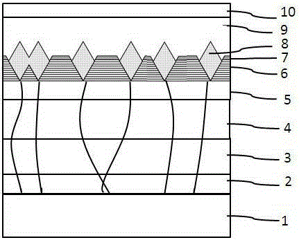
[0039] Please refer to figure 1 and figure 2 , this embodiment provides an LED epitaxial structure, which includes from bottom to top: a substrate 1, a buffer layer 2, a first conductivity type semiconductor layer including a U-GaN layer 3 and an N-GaN layer 4, a superlattice 5, A multi-quantum well layer 6 with a V-shaped pit, an electron blocking layer 7, a double hexagonal hole injection layer 8, a second conductivity type semiconductor layer including a P-GaN layer 9 and a contact layer 10, wherein the double hexagonal hole injection Layer 8 fills the V-shaped pit and embeds the semiconductor layer of the second conductivity type.
[0040] Specifically, the substrate 1 of this embodiment selects sapphire (Al 2 o 3 ), at least one of SiC, GaAs, GaN, ZnO, Si, GaP, InP and Ge, preferably a flat sapphire substrate, although not shown in the figure, the sapphire substrate can also be a patterned sapphire substrate ( PSS), therefore, embodiments are not limited thereto.
...
Embodiment 2
[0048] Please refer to Figure 3~Figure 12 , the present embodiment provides a method for manufacturing an LED epitaxial structure, including the following process steps:
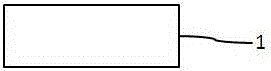
[0049] (1) Please refer to image 3 , provide a substrate 1, can choose sapphire (Al 2 o 3 ), SiC, GaAs, GaN, ZnO, Si, GaP, InP and Ge at least one, preferably a patterned sapphire substrate (PSS).
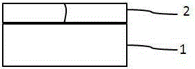
[0050] (2) Please refer to Figure 4 , the buffer layer 2 is epitaxially grown on the substrate 1, preferably InAlGaN semiconductor material, and the epitaxial growth method can be MOCVD (metal organic chemical vapor deposition) method, CVD (chemical vapor deposition) method, PECVD (plasma enhanced chemical vapor deposition) method , MBE (Molecular Beam Epitaxy) method, HVPE (Hydride Vapor Phase Epitaxy) method, preferably MOCVD, but the embodiment is not limited thereto.
[0051] (3) Please refer to Figure 5 On the buffer layer 2, a U-GaN layer 3 and an N-GaN layer 4 are epitaxially grown in sequence to...
Embodiment 3
[0060] Please refer to Figure 13 The difference between this embodiment and embodiment 2 is that in embodiment 2, an electron blocking layer 7 is formed on the top surface of the multi-quantum well layer 6 with V-shaped pits before the hole injection layer 8 is grown, while in the present embodiment After the hole injection layer 8 is grown, a second conductivity type semiconductor layer is grown on the top surface of the multi-quantum well layer 6 with V-shaped pits and the long hole injection layer 8 .
PUM
 Abstract
Description
Claims
Application Information