Optoelectronic device

a technology of optoelectronic devices and optical components, applied in the direction of solid-state devices, semiconductor devices, thermoelectric devices, etc., can solve the problems of device instabilities and/or device failure, thickness and/or contour variations, and device instabilities, etc., to reduce the effect of gaps, reducing the effect of electrical resistance, and reducing the effect of thickness

Active Publication Date: 2015-02-12
CAMBRIDGE DISPLAY TECH LTD
View PDF3 Cites 7 Cited by
  • Summary
  • Abstract
  • Description
  • Claims
  • Application Information

AI Technical Summary

Benefits of technology

[0033]There may further be provided an optoelectronic device in which the first HIL is provided between the anode layer and the one or more further HILs. Thus, a lower conductivity HIL is closer to the semiconducting layer. This may advantageously mitigate the effects of gaps, e.g., pinholes, present within the semiconducting layer by providing higher electrical resistance at localised regions of higher conductivity in the semiconducting, e.g. light emission, layer. Thus, device reliability and / or yield may be enhanced. There may also be provided an optoelectronic device in which the one or more further HILs is provided between the anode layer and the first HIL.
[0034]There may further be provided an optoelectronic device in which the first HIL is adjacent the substrate and has a refractive index which is greater than or equal to or substantially matched to the refractive index of the substrate. The higher conductivity HIL may thus increase conduction between tracks of the anode without significantly impairing device light coupling.
[0035]There may further be provided an optoelectronic device in which the one or more further HILs has a refractive index which is greater than or equal to or substantially matched to the refractive index of the substrate. Preferably, each of the HILs, and more preferably all layers of the device, are substantially index-matched to the substrate to enhance light coupling and thus optoelectronic efficiency of the device.
[0036]There may further be provided an optoelectronic device in which a further layer comprising a hole transport material is provided between the HILs and the semiconductive layer. Such a layer may be referred to as a hole transport layer (HTL). The HTL may have higher hole mobility than electron mobility to increase hole supply to the semiconductive layer, preferably to improve the balance of electron and holes in the semiconductive layer, during operation of the device, thus advantageously improving the optoelectronic efficiency of the device. The hole transport material may be undoped.
[0037]There may further be provided an optoelectronic device in which the first and / or the one or more further HILs are p-doped. The doping concentrations of the HILs may be selected to improve the above alignment of hole energy levels of the semiconductive layer to the hole energy levels of the anode to preferably improve efficiency of hole injection from the anode, thus improving hole transfer between anode and semiconductive layer, and to provide the greater conductivity of the first HIL. Preferably, the first HIL has a conductivity greater than 1 S / cm, preferably greater than 2 S / cm, more preferably greater than 5 S / cm or 10 S / cm. In an embodiment, the conductivity of the first HIL may be greater than that of the second HIL by a factor of, e.g., 2, 10 or 100.

Problems solved by technology

However, deposition of active OLED layers on top of a non-planar surface may result in thickness and / or contour variations, i.e., non-planar surface regions, of the layers.
Such variations may for example result in luminance non-uniformities, device instabilities and / or device failure due to electrical shorts (localised regions of higher current densities (‘hot spots’) for example between the tracks and light emissive layer, or in the light emissive layer) in the device.
However, the sheet resistance of such ITO layer may not be low enough to provide the desired amount and / or uniformity of the luminance of an OLED device.
Moreover, the cost of the ITO material and its deposition process are relatively high and this may be significant in relation to products such as, for example, large area Lighting Panels which may comprise a plurality of OLEDs.
This mismatch in refractive indices between the substrate and the ITO layer can cause optical losses due to light being trapped in waveguided modes.

Method used


Image

  • Optoelectronic device
  • Optoelectronic device
  • Optoelectronic device

Examples


Embodiment Construction

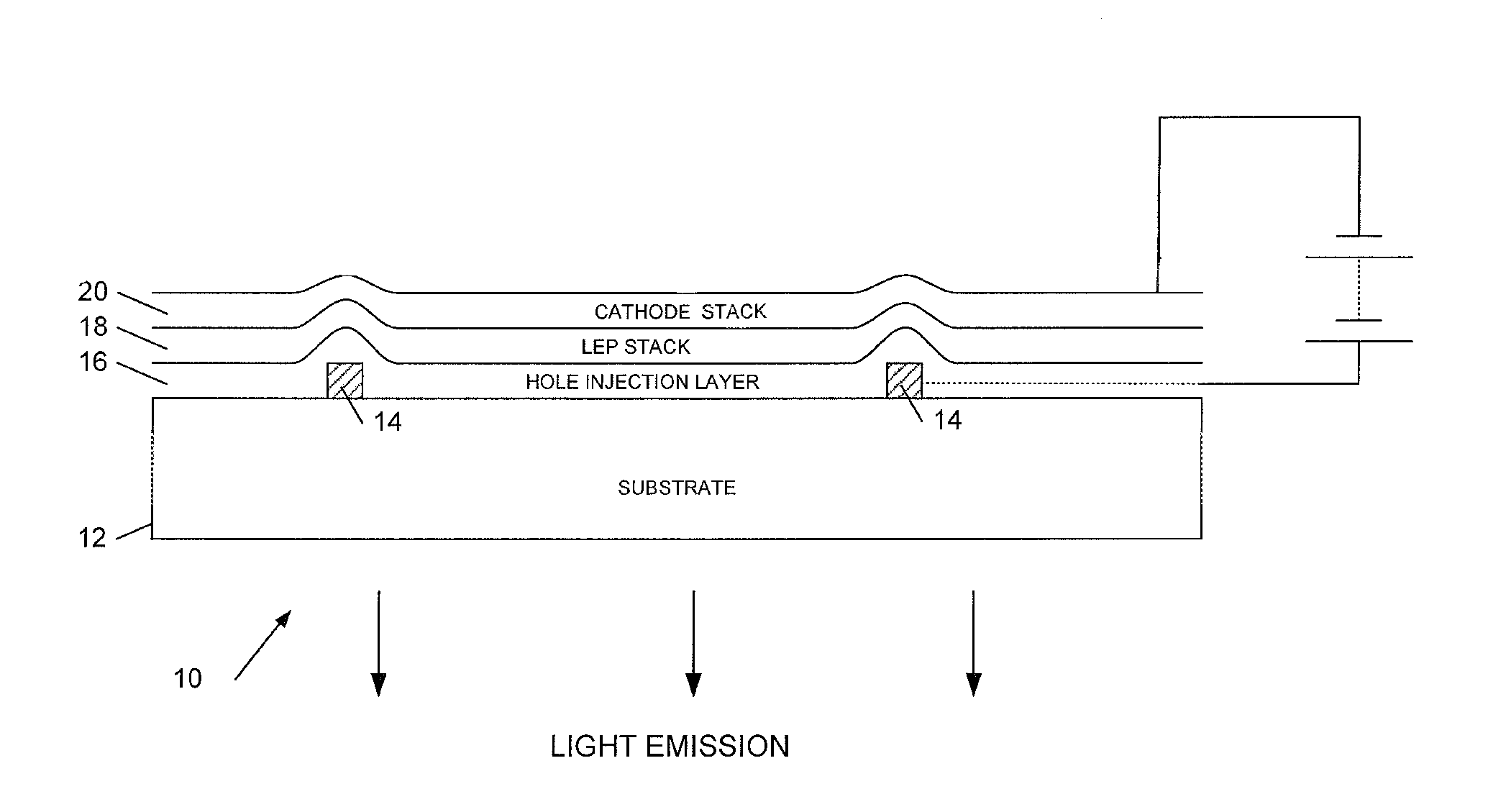
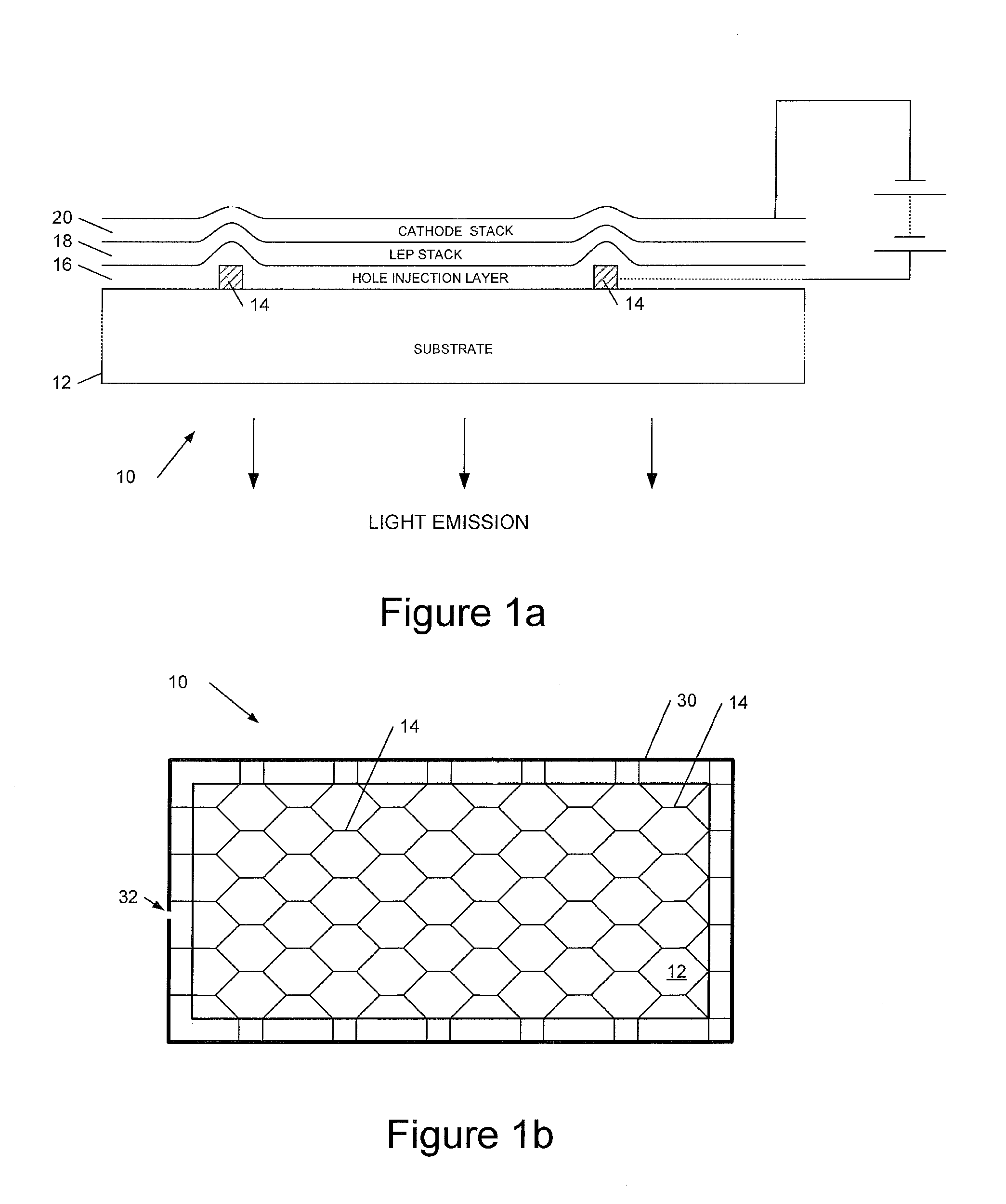
[0057]Embodiments are generally described as optoelectronic devices or methods of fabricating such devices. Merely by way of example, the following refers in the most part to electroluminescent devices, specifically organic light emitting diodes (OLEDs) devices such as a discrete OLED, OLED lighting tile or OLED lighting panel. Nevertheless, it will be apparent to the skilled person that features described below in relation to such devices are similarly applicable to photovoltaic device embodiments.

[0058]FIG. 2 shows an optoelectronic device 28, preferably a bottom-emissive electroluminescent device, comprising anode layer 21 having metal (e.g. comprising copper, gold, silver, aluminium, etc., optionally ink-jet printed, screen printed, electro- or electroless-plated or evaporated) tracks 212 and gaps 211, a plurality of hole injection layers (HILs) comprising a first HIL 23 and a second HIL 24, a semiconductive layer 25, e.g., light emitting polymer (LEP), a cathode layer 26 and a ...


PUM

PropertyMeasurementUnit
conductivityaaaaaaaaaa
thickaaaaaaaaaa
conductivityaaaaaaaaaa

Abstract

This invention generally relates to an optoelectronic device and a method of fabricating such a device, and more particularly to an optoelectronic device comprising an anode layer, a semiconductive layer provided over the anode layer, and a cathode layer provided over the semiconductive layer, the anode layer comprising a plurality of electrically conductive tracks connected together and spaced apart from one another with gaps therebetween, the device further comprising a first and one or more further hole injection layers provided between the anode layer and the semiconductive layer and extending across said gaps, wherein the first hole injection layer has a conductivity greater than the conductivity of the one or more further hole injection layers.

Description

FIELD OF THE INVENTION[0001]The invention generally relates to an optoelectronic device and to a method of fabricating such a device. More specifically, embodiments of the device may, for example, be electroluminescent, such as an organic light emitting diode (OLED) incorporated in a lighting tile, lighting panel, display backlight, or may be photovoltaic.BACKGROUND TO THE INVENTION[0002]Organic light emitting diodes (OLEDs) are particularly useful for lighting because they can be fabricated relatively simply and at low cost to cover a large area on a variety of substrates. They are also bright and may be coloured (red, green and blue) or white as desired. OLEDs may be fabricated using either polymers or small molecules: examples of polymer-based OLEDs are described in WO 90 / 13148, WO 95 / 06400 and WO 99 / 48160; examples of so-called small molecule based devices are described in U.S. Pat. No. 4,539,507. In this specification references to organic LEDs include organometallic LEDs.[0003...

Claims


Application Information

Patent Timeline
Patent Type & Authority Applications(United States)
IPC IPC(8): H01L51/50H01L51/56H01L51/00H01L51/44H01L51/52
CPCH01L51/5088H01L51/441H01L51/5275H01L51/56H01L51/0039H01L51/0038H01L51/0035H10K85/1135H10K30/83H10K50/17H10K50/814Y02E10/549H10K30/81H10K50/858H10K71/00H10K85/111H10K85/114H10K85/115
Inventor MALIK, SURAMACARTER, JULIANSCULLION, LAURENCEBAKER, COLINFLEISSNER, ARNEBURROUGHES, JEREMY
Owner CAMBRIDGE DISPLAY TECH LTD
Why Eureka
Try Eureka