LED epitaxial structure based on h-BN tunnel junction as hole injection layer

A technology of hole injection layer and light-emitting diode, which is applied in the direction of electrical components, circuits, semiconductor devices, etc., can solve the problems of low internal quantum efficiency and restricted efficiency, achieve a large band gap, increase the probability of tunneling, and slow down the current crowding effect of effect

Active Publication Date: 2017-10-24
HEBEI UNIV OF TECH
View PDF7 Cites 6 Cited by
  • Summary
  • Abstract
  • Description
  • Claims
  • Application Information

AI Technical Summary

Problems solved by technology

In deep ultraviolet LEDs, the problem of doping efficiency of p-AlGaN material is very prominent. If p-GaN layer is used, its doping efficiency is improved compared with p-AlGaN layer, but due to the activation energy of Mg at room temperature As high as 180meV, the highest activation rate is only 1%, which seriously restricts the efficiency of hole injection from the p-type electrode into the quantum well of the device, and finally leads to its internal quantum efficiency lower than 60%.

Method used


Image

  • LED epitaxial structure based on h-BN tunnel junction as hole injection layer
  • LED epitaxial structure based on h-BN tunnel junction as hole injection layer
  • LED epitaxial structure based on h-BN tunnel junction as hole injection layer

Examples


Embodiment 1

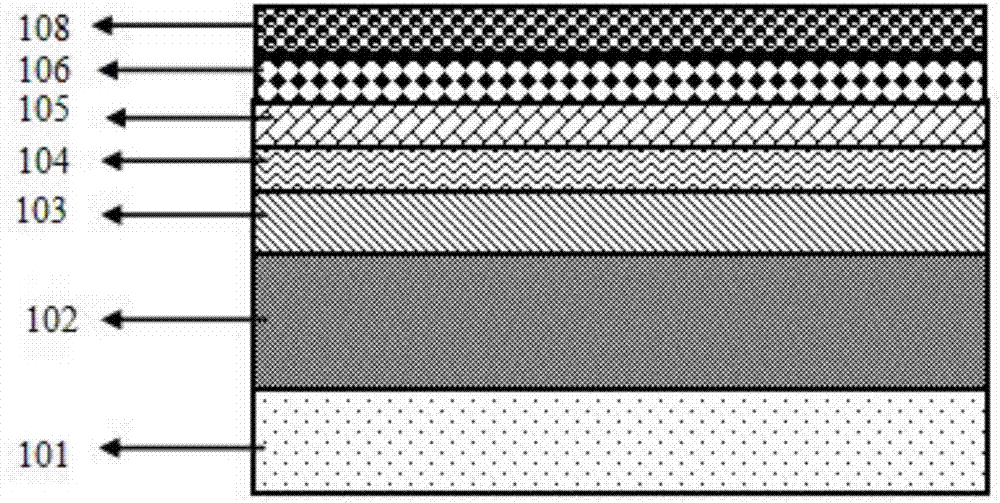
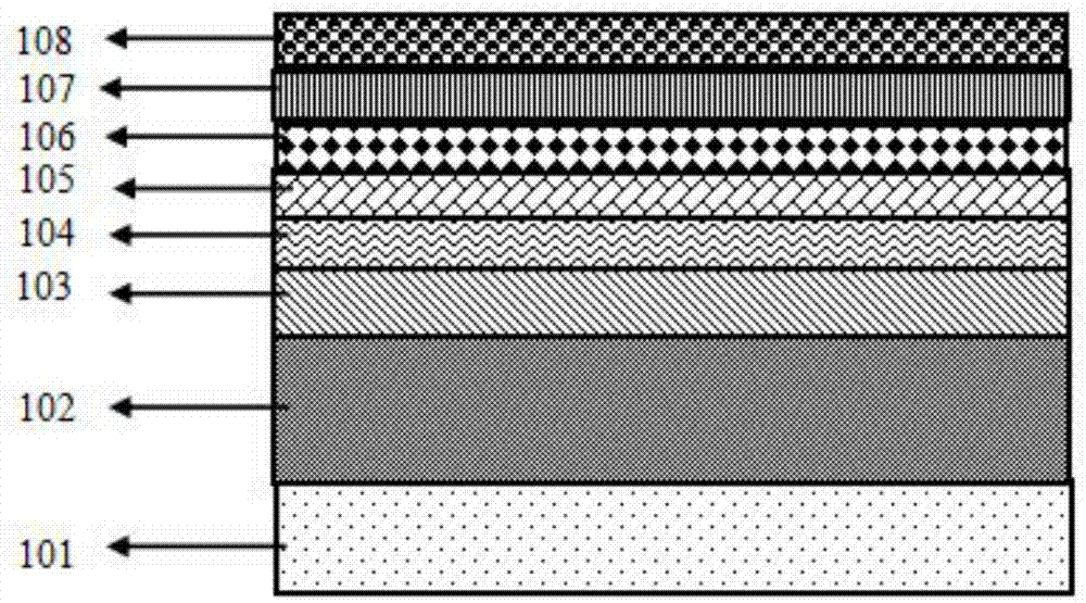
[0046] This embodiment is based on the light-emitting diode epitaxial structure (referred to as the epitaxial structure, see figure 2 ) includes substrate 101, n-type semiconductor material layer 102, multiple quantum well layer 103, p-type electron blocking layer 104, p-type semiconductor material layer 105, p-type heavily doped semiconductor material layer 106, h-BN layer 107 and an n-type heavily doped semiconductor material layer 108, wherein the relative permittivity of the h-BN layer is 4, which is smaller than the relative permittivity and n of the p-type heavily doped semiconductor material layer 106 -type heavily doped semiconductor material layer 108; the p-type heavily doped semiconductor material layer 106, h-BN layer 107 and n-type heavily doped semiconductor material layer 108 together form a tunnel junction.

[0047] Wherein, the doping element concentration of the n-type heavily doped semiconductor material layer 108 needs to be not less than that of the n-typ...

Embodiment 2

[0062] The composition and preparation method of each part of the epitaxial structure in this embodiment are the same as in Embodiment 1, except that the substrate 101 described in this embodiment is AlN, which is [0001] polar; the material of the n semiconductor material layer 102 is Al 0.60 Ga 0.40 N, with a thickness of 400nm; the structure of the multi-quantum well layer 103 is Al 0.45 Ga 0.55 N / Al 0.60 G a0.40 N, where the quantum barrier Al 0.60 G a0.40 The thickness of N is 10nm, the quantum well Al 0.45 Ga 0.55 The thickness of N is 3nm, the number of quantum wells is 7; the p-type electron blocking layer 104 is made of Al0.65 Ga 0.35 N thickness is 20nm; p-type semiconductor material layer 105 is made of Al 0.40 Ga 0.60 N, with a thickness of 200nm; the material of the p-type heavily doped semiconductor material layer is GaN, with a thickness of 20nm; the thickness of the h-BN layer 107 is 3nm, and the relative dielectric constant of the h-BN layer is 5.1, n...


PUM


Abstract

The invention relates to an LED epitaxial structure based on an h-BN tunnel junction as a hole injection layer. The invention is characterized in that the epitaxial structure comprises a substrate, an n-type semiconductor material layer, a multi-quantum well layer, a p-type electronic blocking layer, a p-type semiconductor material layer, a p-type heavily doped semiconductor material layer, an h-BN layer and an n-type heavily doped semiconductor material layer, the relative dielectric constant of the n-BN layer is 3-5.1, the relative dielectric constant is less than the relative dielectric constant of the p-type heavily doped semiconductor material layer and the n-type heavily doped semiconductor material layer, the thickness of the h-BN layer is 1nm-5nm; and the p-type heavily doped semiconductor material layer, the h-BN layer and the n-type heavily doped semiconductor material layer constitute a tunnel junction together. The LED epitaxial structure has a tunnel junction structure capable of improving the hole injection efficiency of an LED device, thereby increasing the tunneling probability of carriers, improving the current expansion effect, and significantly improving the quantum efficiency and light output power in the LED.

Description

technical field [0001] The technical solution of the present invention relates to the technical field of semiconductor devices, specifically a light-emitting diode epitaxial structure based on h-BN tunneling junction as a hole injection layer. In the epitaxial structure, the p-type heavily doped semiconductor material layer, the h-BN layer and the n-type heavily doped semiconductor material layer jointly form a tunnel junction to enhance the electric field. Background technique [0002] Group-III nitride materials have been widely used in the field of optoelectronic devices, one of the important applications is light-emitting diodes (LEDs). The light-emitting diodes of III-V nitrides can be widely used in lighting, display and other fields, and have reached a very high level in the field of blue light. At present, further research is being carried out in the ultraviolet band, which has unique advantages in the fields of inspection, sterilization, polymer curing, and biochem...

Claims


Application Information

Patent Timeline
Patent Type & Authority Applications(China)
IPC IPC(8): H01L33/14H01L33/06H01L33/00
CPCH01L33/0075H01L33/06H01L33/14
Inventor 李路平田康凯楚春双张勇辉毕文刚张紫辉
Owner HEBEI UNIV OF TECH
Why Eureka
Try Eureka