Eureka AIR delivers breakthrough ideas for toughest innovation challenges, trusted by R&D personnel around the world.

Vertically stacked gate-all-around silicon nanowire tunneling field-field transistor and preparation method thereof

A technology of tunneling field effect and vertical stacking, which is applied in the direction of nanotechnology, nanotechnology, nanotechnology, etc. for materials and surface science, and can solve the problems that it is difficult to improve the bidirectional conduction characteristics of the opening current of tunneling field effect transistors. Achieve the effects of suppressing bidirectional conduction characteristics, increasing the effective tunneling area, and increasing the turn-on current

Active Publication Date: 2018-06-08
INST OF MICROELECTRONICS CHINESE ACAD OF SCI
View PDF5 Cites 3 Cited by
  • Summary
  • Abstract
  • Description
  • Claims
  • Application Information

AI Technical Summary

Problems solved by technology

[0004] The main purpose of the present invention is to provide a vertically stacked gate-all-around nanowire tunneling field effect transistor and its preparation method to solve the problems in the prior art that it is difficult to improve the turn-on current of the tunneling field effect transistor and suppress its bidirectional conduction characteristics question

Method used


Image

  • Vertically stacked gate-all-around silicon nanowire tunneling field-field transistor and preparation method thereof
  • Vertically stacked gate-all-around silicon nanowire tunneling field-field transistor and preparation method thereof
  • Vertically stacked gate-all-around silicon nanowire tunneling field-field transistor and preparation method thereof

Examples


Embodiment Construction

[0105] It should be noted that the embodiments of the present invention and the features of the embodiments may be combined with each other under the condition of no conflict. The present invention will be described in detail below with reference to the accompanying drawings and in conjunction with the embodiments.

[0106] In order to make those skilled in the art better understand the solutions of the present invention, the technical solutions in the embodiments of the present invention will be clearly and completely described below with reference to the accompanying drawings in the embodiments of the present invention. Obviously, the described embodiments are only Embodiments are part of the present invention, but not all embodiments. Based on the embodiments of the present invention, all other embodiments obtained by persons of ordinary skill in the art without creative efforts shall fall within the protection scope of the present invention.

[0107] It should be noted th...


PUM


Abstract

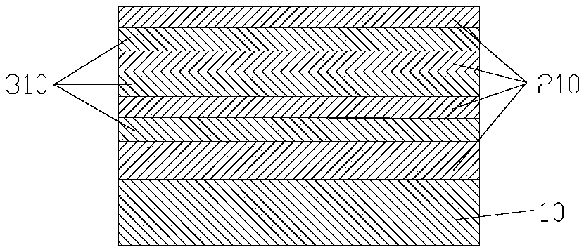
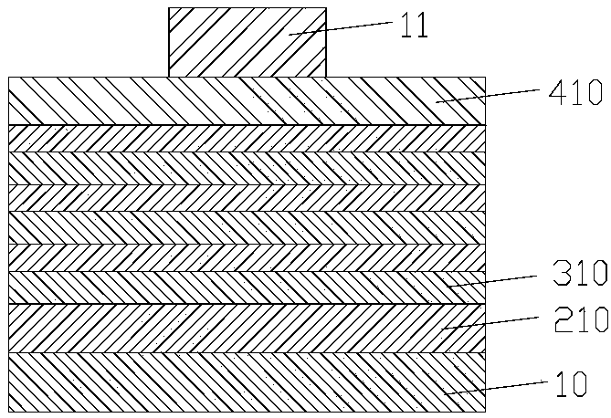
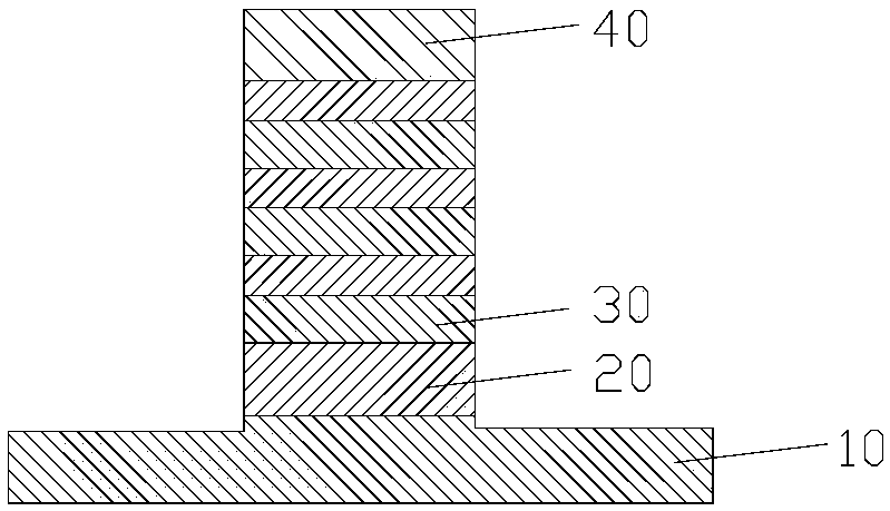
The invention provides a vertically stacked gate-all-around silicon nanowire tunneling field-field transistor and a preparation method thereof. The preparation method comprises: a nanowire array and agate stacking structure surrounding the nanowire array are formed, wherein a first notch and a second notch that correspond to each other are formed at the two ends of the gate stacking structure; ahigh-k medium side wall and a low-k medium side wall are formed in the first notch and the second notch respectively; and a heavily-doped layer is formed between the high-k medium side wall and a channel layer. Because the heavily-doped layer having the type opposite to the doping type of a source region is inserted between the source region and the channel layer, the tunneling probability is increased; on the basis of the gate-all-around structure, the gate control capability is enhanced; the local electrical field is increased by introducing the high-k medium side wall into one side of the source region; with the gate-all-around nanowires stacked in a vertical direction, the effective tunneling area is extended and thus the opening current of the tunneling field-field transistor is improved obviously; and because of the low-k medium side wall at one side of the drain region, the bidirectional conduction characteristics of the tunneling field effect transistor are suppressed effectively.

Description

technical field [0001] The invention relates to the technical field of semiconductors, and in particular, to a vertically stacked ring gate nanowire tunneling field effect transistor and a preparation method thereof. Background technique [0002] With the improvement of the integration density of CMOS devices, the increasing power consumption will become an important bottleneck restricting the further development of integrated circuits. Reducing the operating voltage by reducing the sub-threshold swing of the device is an effective solution to reduce power consumption, and tunneling field effect transistors are one of the effective technical routes to achieve this solution. However, the tunneling field effect transistor has a low turn-on current, which makes it easy to conduct bidirectional conduction. [0003] Improving the turn-on current and suppressing the bidirectional conduction characteristics of the tunneling field effect transistor by optimizing the device structur...

Claims


Application Information

Patent Timeline
IPC IPC(8): H01L29/739H01L21/331H01L29/10B82Y30/00
CPCB82Y30/00H01L29/1025H01L29/66356H01L29/7391
Inventor 朱正勇朱慧珑
Owner INST OF MICROELECTRONICS CHINESE ACAD OF SCI
Why Eureka
Eureka Blog
Learn More