

Semiconductor device and making method thereof
A technology of semiconductors and nitride semiconductors, which is applied in semiconductor/solid-state device manufacturing, semiconductor devices, electrical components, etc., can solve problems such as high resistance and lower frequency response characteristics of devices, so as to reduce peak electric field, reduce current collapse effect, reduce The effect of current collapse
- Summary
- Abstract
- Description
- Claims
- Application Information
AI Technical Summary
Problems solved by technology
Method used
Image

Examples
Embodiment 1
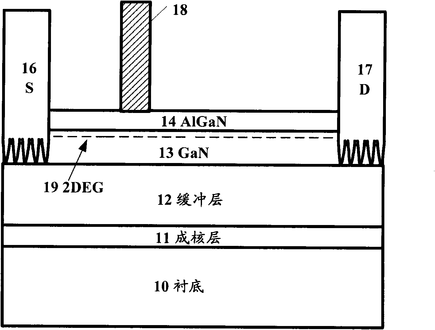
[0070] Figure 4 A device structure of a semiconductor device according to an embodiment of the present invention is shown.
[0071] First refer to the following Figure 4 The basic structure of a gallium nitride HEMT as an example of a semiconductor device of this embodiment will be described.
[0072] Such as Figure 4 As shown, the bottom layer is a substrate (also referred to as a substrate or substrate) 10 for growing gallium nitride material, and the substrate 10 is generally sapphire (Sapphire), SiC, GaN, Si or any other known to those skilled in the art. Any substrate or substrate suitable for growing gallium nitride material is not limited by the present invention.
[0073] On the substrate 10 is an optional nucleation layer 11 for growing a semiconductor layer thereon. It should be understood that the semiconductor layer may be directly formed on the substrate 10 without forming the nucleation layer 11 .
[0074] On the nucleation layer 11 is a buffer layer 12 o...
Embodiment 2
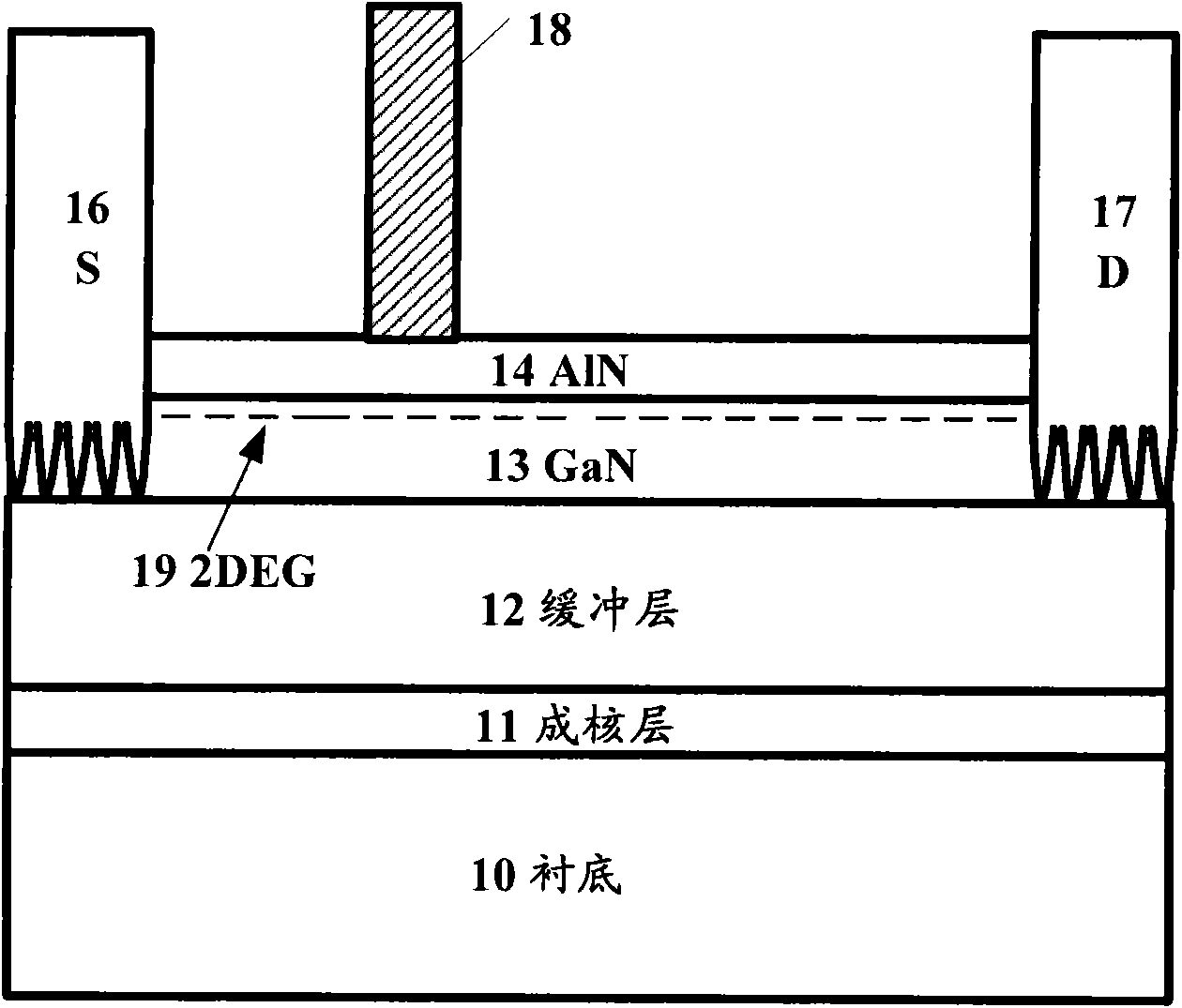
[0091] Figure 5 A device structure of a semiconductor device according to another embodiment of the present invention is shown.
[0092] Such as Figure 5 As shown, this embodiment is the same as the above Figure 4 The difference of Embodiment 1 is that no passivation layer 20 is formed between the gate 18 and the n-type doped layer 15 . The description of the same parts of Embodiment 2 as Embodiment 1 is omitted here, and the differences between the two will be described below.
[0093] In Embodiment 1, there is a passivation layer between the gate 18 and the n-type doped layer 15 . In this design, the process needs to be optimized to obtain a passivation layer with a high breakdown electric field, otherwise the breakdown voltage of the device will be limited by the passivation layer.
[0094] In this embodiment, the passivation layer 20 between the gate 18 and the n-type doped layer 15 is removed, as Figure 5 As shown, the gate 18 and the n-type doped layer 15 are se...
Embodiment 3
[0096] Image 6 A device structure of a semiconductor device according to another embodiment of the present invention is shown.
[0097] Such as Image 6 As shown, this embodiment is the same as the above Figure 5 The only difference of the second embodiment is that there is a dielectric layer 21 between the gate 18 and the isolation layer 15 . The description of the same parts of Embodiment 3 as Embodiment 2 is omitted here, and the differences between the two will be described below.
[0098] In Example 2 of Figure 5 In the shown structure, the AlN isolation layer 14 is very thin, and electrons easily tunnel from the channel into the gate 18, resulting in a large gate leakage current. Based on a modification of the present invention, the form of an insulating gate can also be used, such as Image 6 shown. Dielectric layer 12 can adopt SiN, SiO 2 or other insulating media. The insulating gate forms a potential barrier between the metal and the electronic channel, wh...
PUM
 Abstract
Description
Claims
Application Information