Method of forming shallow trench isolation structure

a technology of isolation structure and shallow trench, which is applied in the direction of semiconductor/solid-state device manufacturing, basic electric elements, electric devices, etc., can solve the problems of difficult and complicated fabrication of such dual isolation structures having different depths

Active Publication Date: 2015-01-15
UNITED MICROELECTRONICS CORP
View PDF1 Cites 31 Cited by
  • Summary
  • Abstract
  • Description
  • Claims
  • Application Information

AI Technical Summary

Benefits of technology

[0007]Accordingly, the present invention provides a method of forming a shallow trench isolation structure, which successfully integrates the dual isolation structures into the existing CMOS process.

Problems solved by technology

However, it has been difficult and complicated to fabricate such dual isolation structures having different depths.

Method used


Image

  • Method of forming shallow trench isolation structure
  • Method of forming shallow trench isolation structure
  • Method of forming shallow trench isolation structure

Examples


first embodiment

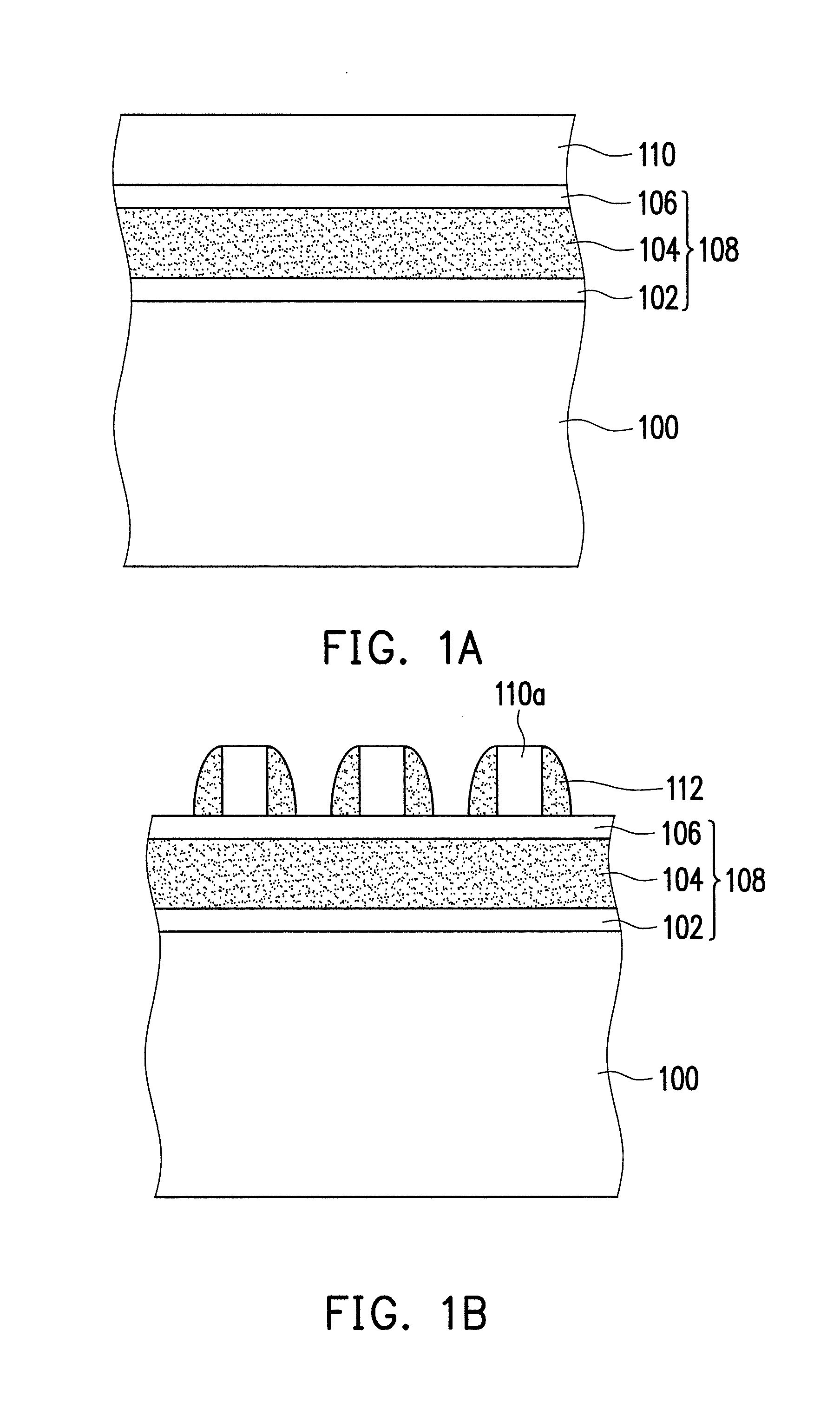
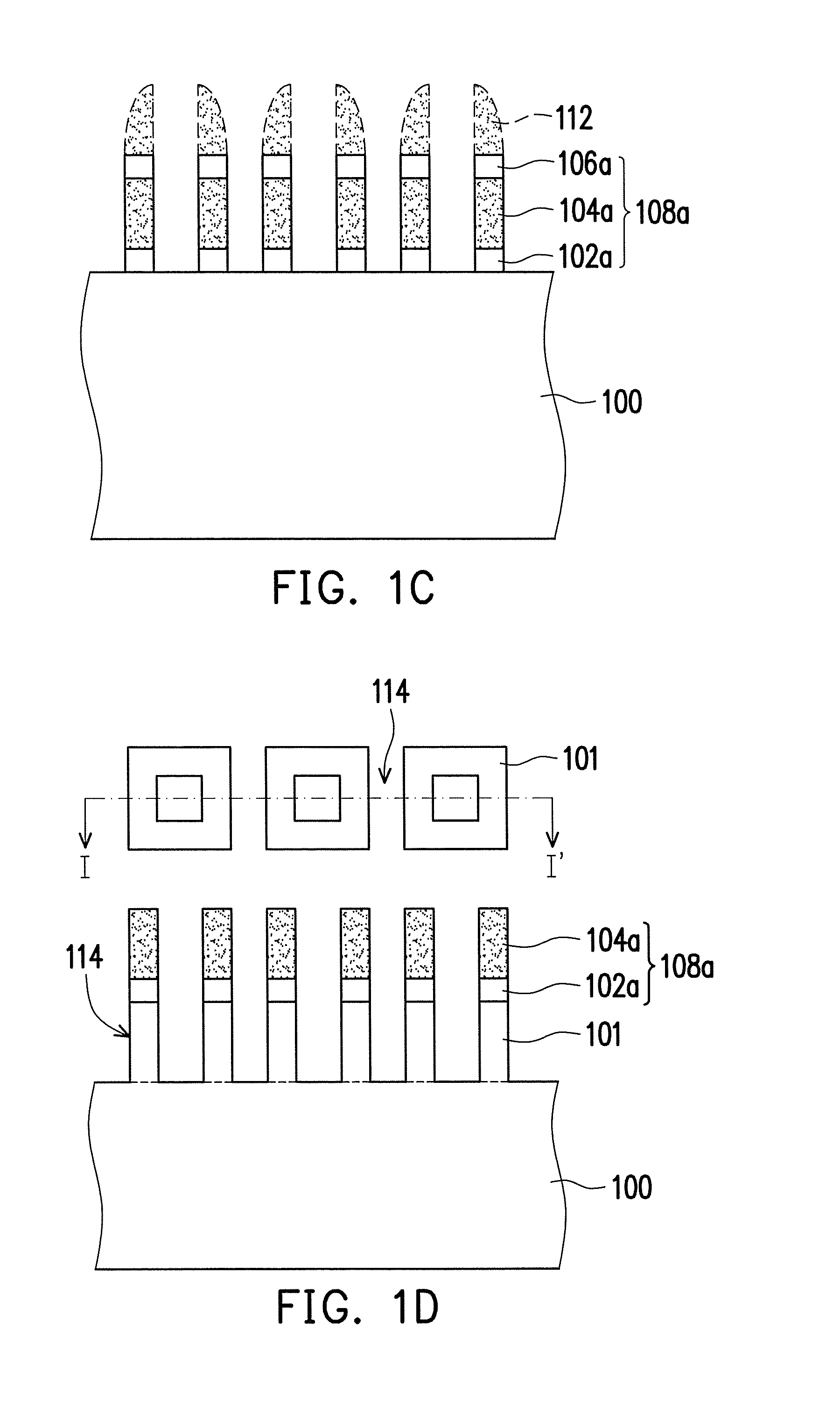
[0035]FIG. 1A to FIG. 1J are schematic cross-sectional views illustrating a method of forming a shallow trench isolation structure according to a first embodiment of the present invention. It is noted that each of FIG. 1D to FIG. 1F has two parts in the drawing, the lower part illustrates a cross-sectional view, and the upper part illustrates a top view. For clarity and convenience of illustration, some components are omitted from the top views in FIG. 1D to FIG. 1F.

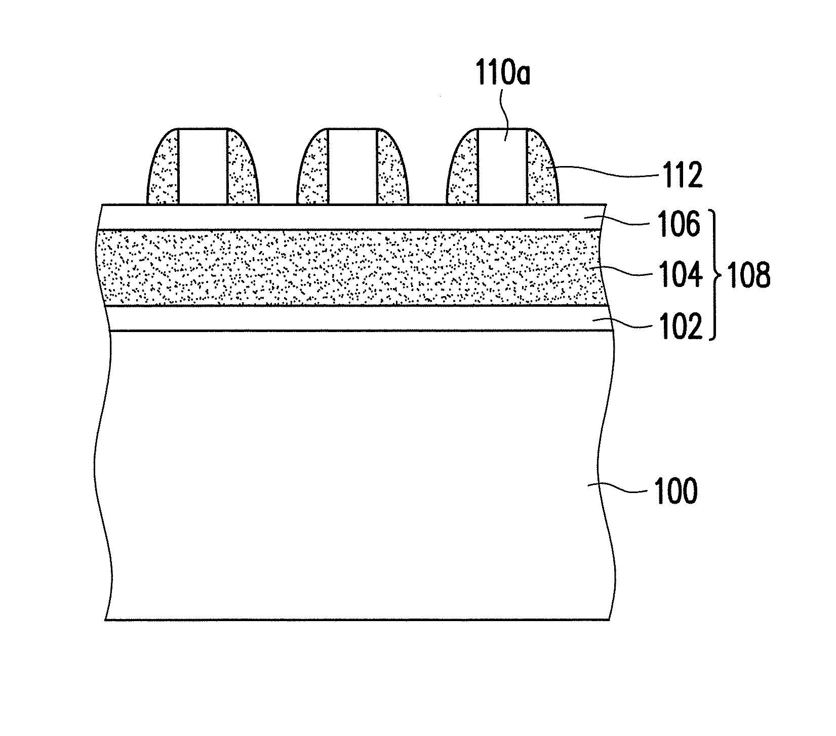
[0036]Referring to FIG. 1A, a hard mask layer 108 and a sacrificial layer 110 are sequentially formed on the substrate 100. The substrate 100 can be a semiconductor substrate, such as a silicon-containing substrate. The hard mask layer 108 can be a single layer or a multi-layer structure. In this embodiment, the hard mask layer 108 includes, from bottom to top, a first oxide layer 102, a nitride layer 104 and a second oxide layer 106. The first oxide layer 102 includes silicon oxide. The nitride layer 104 includes silico...

second embodiment

[0052]FIG. 2A to FIG. 2G are schematic cross-sectional views illustrating a method of forming a shallow trench isolation structure according to a second embodiment of the present invention. The second embodiment is similar to the first embodiment, the difference between them is illustrated in the following, and the similarities are not iterated herein.

[0053]Referring to FIG. 2A, first, the intermediate structure of FIG. 1D is provided. A filling layer 200 is formed in the first trenches 114. The insulating layer as a filling layer 200 can be blanket-formed on the substrate 100 filling in the first trenches 114 through a suitable deposition (FCVD) or spin-coating process. In an embodiment, the filling layer 200 can be an insulating layer including silicon oxide or a suitable dielectric material formed through a CVD process. In another embodiment, the filling layer 200 can be a softer insulating layer or a spin-on dielectric (SOD) material to have a substantially planar top surface.

[0...


PUM


Abstract

A method of forming a shallow trench isolation structure is disclosed. Hard mask patterns are formed on a substrate. A portion of the substrate is removed, using the hard mask patterns as a mask, to form first trenches in the substrate, wherein a fin is disposed between the neighboring first trenches. A filling layer is formed in the first trenches. A patterned mask layer is formed on the filling layer. A portion of the filling layer and a portion of the fins are removed, using the patterned mask layer as a mask, to form second trenches in the substrate. A first insulating layer is formed on the substrate filling in the second trenches.

Description

BACKGROUND OF THE INVENTION[0001]1. Field of Invention[0002]The present invention relates to a semiconductor process, and more particularly to a method of forming a shallow trench isolation structure.[0003]2. Description of Related Art[0004]As the device dimension continues to shrink and the level of integration continues to increase, a structure for isolating devices is required to reduce accordingly.[0005]Since a shallow trench isolation (STI) structure is scalable without causing any bird's beak encroachment problem as in the conventional local oxidation of silicon (LOCOS) process, it is the preferred isolation technique for a sub-micron (or smaller dimension) metal-oxide-semiconductor fabrication process.[0006]In addition, the required depths of isolation structures are varied according to different applications in the same chip. For example, in a fin-type field effect transistor (FinFET) device, the depth of a STI structure for fins may be different from that for well regions. ...

Claims


Application Information

Patent Timeline
Patent Type & Authority Applications(United States)
IPC IPC(8): H01L21/762
CPCH01L21/76224H01L21/308H01L21/3086H01L21/823431H01L21/823821H01L21/823878H01L21/845
Inventor LIN, CHIEN-TINGTSAI, SHIH-HUNGLIN, CHUN-HSIEN
Owner UNITED MICROELECTRONICS CORP
Why Eureka
Try Eureka