
Adhesive wafer bonding with controlled thickness variation

Active Publication Date: 2015-01-29
APPLE INC
View PDF3 Cites 82 Cited by
  • Summary
  • Abstract
  • Description
  • Claims
  • Application Information

AI Technical Summary

Benefits of technology

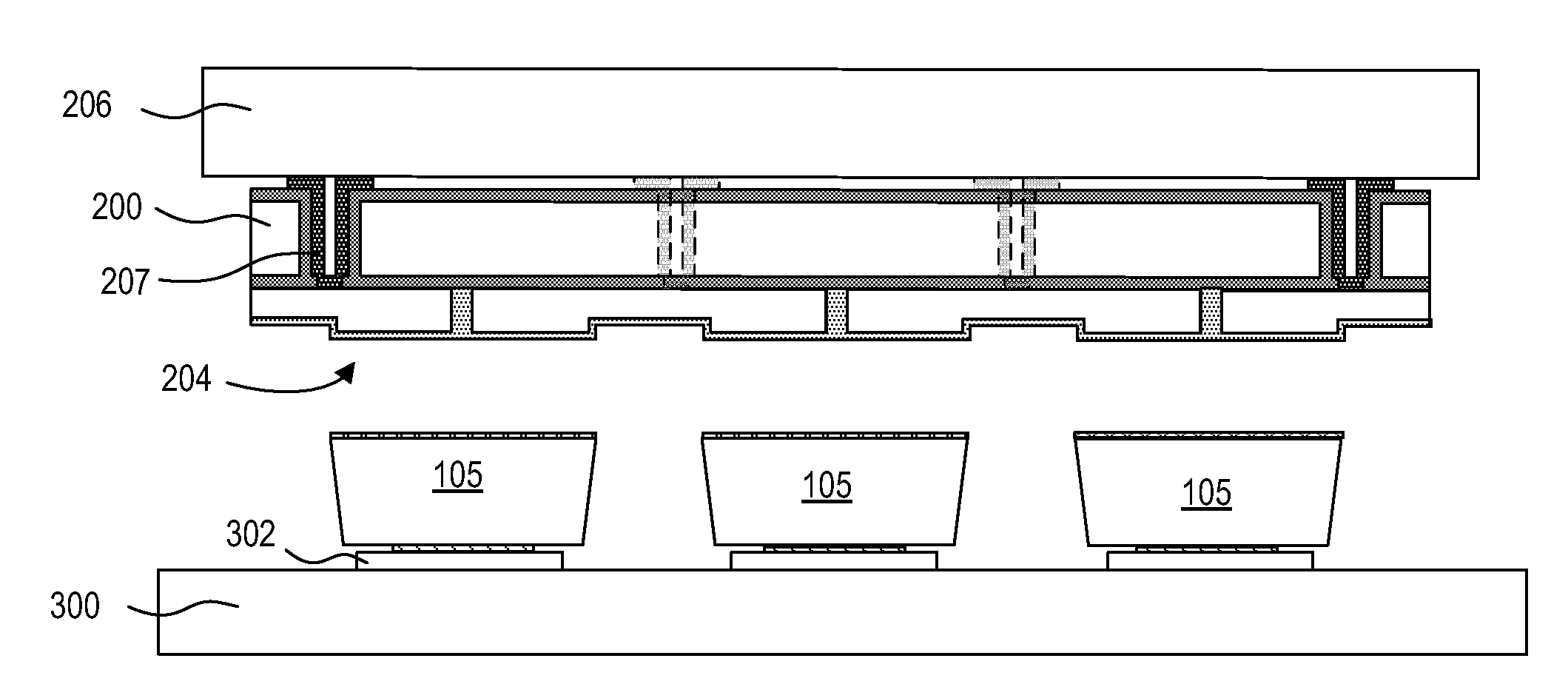
The patent describes a process for making a micro device mesa structure on a handle substrate. A sacrificial layer is patterned and then a stabilization layer is formed on top of it. This layer is then bonded to a carrier substrate with raised spacers. An adhesion promoter layer is used to improve adhesion between the carrier substrate and the stabilization layer. The technical effect of this process is to provide a way to create a reliable and reliable connection between a micro device and a carrier substrate for further processing and functionality.

Problems solved by technology

Commercial manufacturing and packaging of micro devices often becomes more challenging as the scale of the micro devices decreases.

Method used


Image

  • Adhesive wafer bonding with controlled thickness variation
  • Adhesive wafer bonding with controlled thickness variation
  • Adhesive wafer bonding with controlled thickness variation

Examples


Embodiment Construction

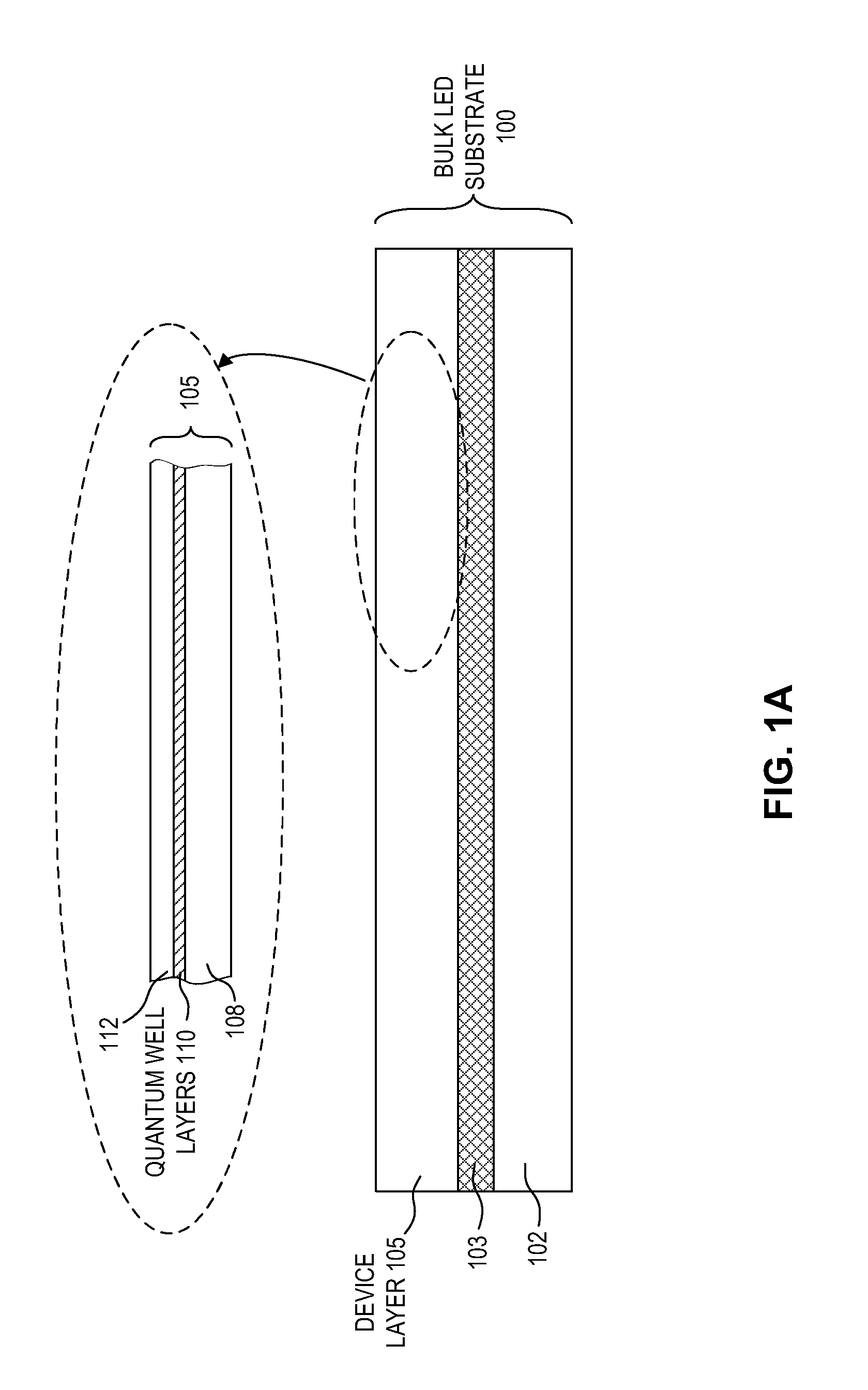
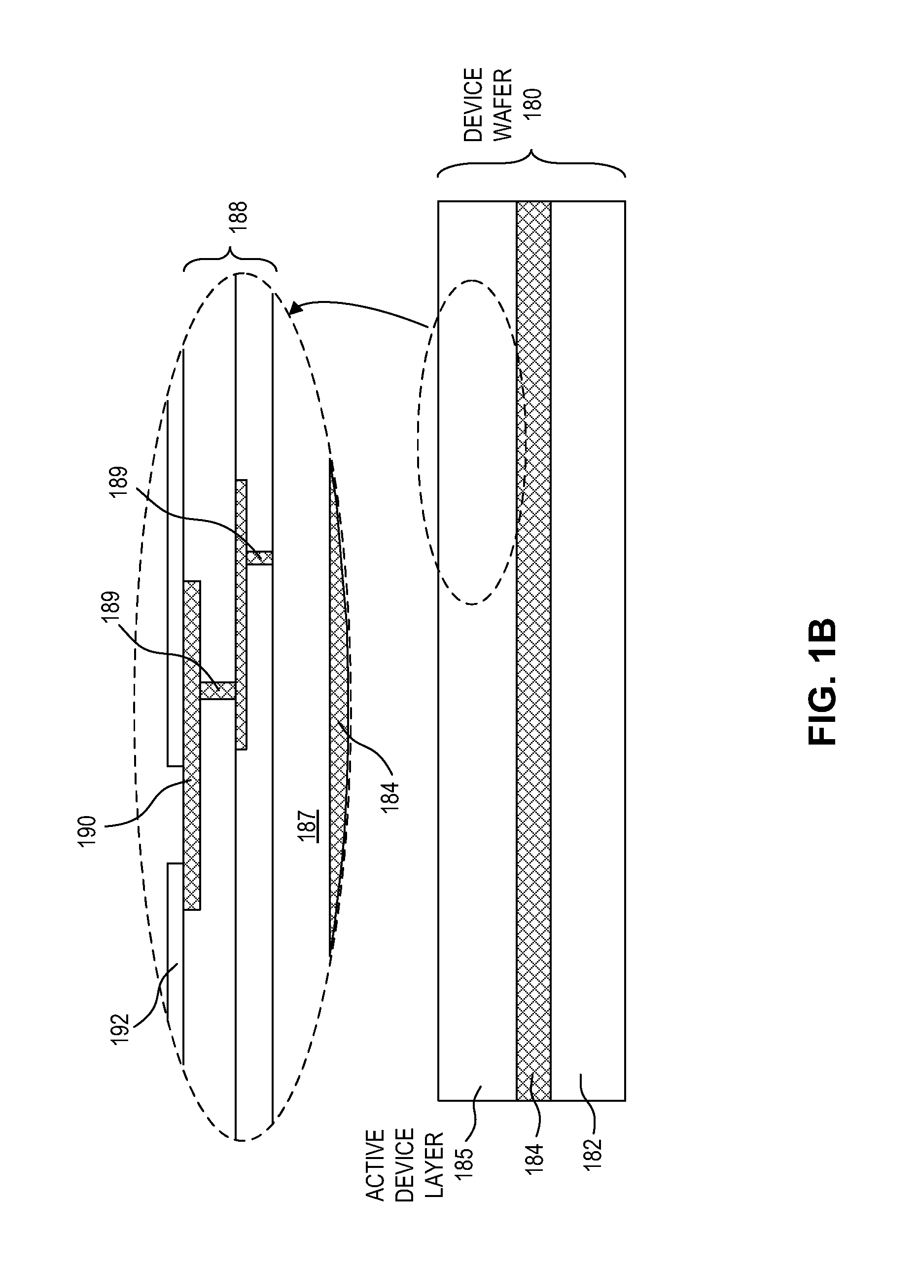
[0035]Embodiments of the present invention describe a method and structure for stabilizing an array of micro devices such as micro light emitting diode (LED) devices and micro chips on a carrier substrate having raised spacers so that they are poised for pick up and transfer to a receiving substrate. For example, the receiving substrate may be, but is not limited to, a display substrate, a lighting substrate, a substrate with functional devices such as transistors or integrated circuits (ICs), or a substrate with metal redistribution lines. While embodiments of some of the present invention are described with specific regard to micro LED devices comprising p-n diodes, it is to be appreciated that embodiments of the invention are not so limited and that certain embodiments may also be applicable to other micro semiconductor devices which are designed in such a way so as to perform a predetermined electronic function (e.g. diode, transistor, integrated circuit) or photonic function (L...


PUM


Abstract

A method and structure for forming an array of micro devices is disclosed. An array of micro devices is formed over an array of stabilization posts included in a stabilization layer. The stabilization layer is bonded to a spacer side of a carrier substrate. The spacer side of the carrier substrate includes raised spacers extending from a spacer-side surface of the carrier substrate.

Description

BACKGROUND[0001]1. Field[0002]The present invention relates to micro devices. More particularly embodiments of the present invention relate to the stabilization of micro devices on a carrier substrate.[0003]2. Background Information[0004]Commercial manufacturing and packaging of micro devices often becomes more challenging as the scale of the micro devices decreases. Some examples of micro devices include radio frequency (RF) microelectromechanical systems (MEMS) microswitches, light-emitting diode (LED) display systems, and MEMS or quartz-based oscillators.[0005]During fabrication of active devices, it is common to include bonding together two wafers or substrates. For example, a growth substrate may be bonded with a carrier substrate to position the device structure on a different wafer or substrate in order to perform processing operations on an alternate side of the micro device structure. The growth substrate may also be bonded with a carrier substrate because the carrier subst...

Claims


Application Information

Patent Timeline
IPC IPC(8): H01L27/15H01L33/00H01L33/06
CPCH01L27/156H01L33/005H01L33/06H01L24/05H01L24/29H01L24/75H01L24/83H01L24/95H01L2224/05139H01L2224/05155H01L2224/05166H01L2224/05169H01L2224/05609H01L2224/05611H01L2224/05613H01L2224/05639H01L2224/05644H01L2224/29117H01L2224/29138H01L2224/29144H01L2224/29155H01L2224/29186H01L2224/2919H01L2224/75252H01L2224/7598H01L2224/83192H01L2224/83409H01L2224/83411H01L2224/83444H01L2224/8349H01L2224/83815H01L2224/8382H01L2224/83895H01L2924/10155H01L2924/12041H01L2924/12042H01L2924/1461H01L33/0093H01L2924/00H01L2924/00012H01L2924/00014H01L2924/014H01L2924/013H01L2924/01004H01L2924/01028H01L2924/053H01L2924/01032H01L2924/01079H01L2924/0665H01L24/00
Inventor CHAN, CLAYTON KA TSUNBIBL, ANDREAS
Owner APPLE INC
Learn More